ZHCSSI1D august   2008  – august 2023 DAC5311 , DAC6311 , DAC7311

PRODUCTION DATA  

  1.   1
  2. 特性
  3. 应用
  4. 说明
  5. Revision History
  6. Device Comparison
  7. Pin Configuration and Functions
  8. Specifications
    1. 7.1  Absolute Maximum Ratings
    2. 7.2  ESD Ratings
    3. 7.3  Recommended Operating Conditions
    4. 7.4  Thermal Information
    5. 7.5  Electrical Characteristics
    6. 7.6  Timing Requirements
    7. 7.7  Timing Diagrams
    8. 7.8  Typical Characteristics: AVDD = 5 V
    9. 7.9  Typical Characteristics: AVDD = 3.6 V
    10. 7.10 Typical Characteristics: AVDD = 2.7 V
  9. Detailed Description
    1. 8.1 Overview
    2. 8.2 Functional Block Diagram
    3. 8.3 Feature Description
      1. 8.3.1 DAC Section
      2. 8.3.2 Resistor String
      3. 8.3.3 Output Amplifier
      4. 8.3.4 Power-On Reset
    4. 8.4 Device Functional Modes
      1. 8.4.1 Power-Down Modes
    5. 8.5 Programming
      1. 8.5.1 Serial Interface
        1. 8.5.1.1 Input Shift Register
        2. 8.5.1.2 SYNC Interrupt
  10. Application and Implementation
    1. 9.1 Application Information
      1. 9.1.1 Microprocessor Interfacing
        1. 9.1.1.1 DACx311 to 8051 Interface
        2. 9.1.1.2 DACx311 to Microwire Interface
        3. 9.1.1.3 DACx311 to 68HC11 Interface
    2. 9.2 Typical Applications
      1. 9.2.1 Loop Powered Transmitter
        1. 9.2.1.1 Design Requirements
        2. 9.2.1.2 Detailed Design Procedure
        3. 9.2.1.3 Application Curves
      2. 9.2.2 Using the REF5050 as a Power Supply for the DACx311
      3. 9.2.3 Bipolar Operation Using the DACx311
    3. 9.3 Power Supply Recommendations
    4. 9.4 Layout
      1. 9.4.1 Layout Guidelines
      2. 9.4.2 Layout Example
  11. 10Device and Documentation Support
    1. 10.1 接收文档更新通知
    2. 10.2 支持资源
    3. 10.3 Trademarks
    4. 10.4 静电放电警告
    5. 10.5 术语表
  12. 11Mechanical, Packaging, and Orderable Information

Application Curves

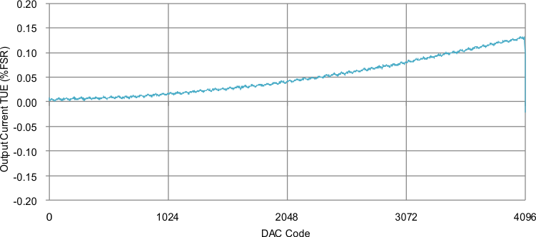
Figure 9-6 shows the measured transfer function of the circuit. Figure 9-7 shows the total unadjusted error (TUE) of the circuit, staying below 0.15 %FSR.
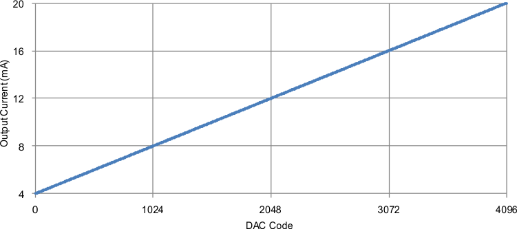
GUID-0AE14AA7-C9E3-49FC-8FCE-BEB911DA8DB0-low.gifFigure 9-6 Output Current vs Code
GUID-92B7CD55-8FF9-4897-9803-E5D7BBA32BFB-low.gifFigure 9-7 Current Total Unadjusted Error vs Code