ZHCSTS6K December 2003 – November 2023 SN74AVC8T245
PRODUCTION DATA
- 1
- 1 特性
- 2 应用
- 3 说明
- 4 Pin Configuration and Functions
-
5 Specifications
- 5.1 Absolute Maximum Ratings
- 5.2 ESD Ratings
- 5.3 Recommended Operating Conditions
- 5.4 Thermal Information
- 5.5 Electrical Characteristics
- 5.6 Switching Characteristics, VCCA = 1.2 V
- 5.7 Switching Characteristics, VCCA = 1.5 V ± 0.1 V
- 5.8 Switching Characteristics, VCCA = 1.8 V ± 0.15 V
- 5.9 Switching Characteristics, VCCA = 2.5 V ± 0.2 V
- 5.10 Switching Characteristics, VCCA = 3.3 V ± 0.3 V
- 5.11 Operating Characteristics
- 5.12 Typical Total Static Power Consumption (ICCA + ICCB)
- 5.13 Typical Characteristics
- Parameter Measurement Information
- 6 Detailed Description
- 7 Application and Implementation
- 8 Device and Documentation Support
- 9 Revision History
- 10Mechanical, Packaging, and Orderable Information
4 Pin Configuration and Functions
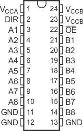
 Figure 4-1 DGV or PW Package, 24-Pin
TVSOP or TSSOP (Top View)
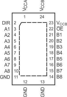
 Figure 4-2 RHL Package, 24-Pin VQFN
(Top View)
Figure 4-2 RHL Package, 24-Pin VQFN
(Top View)Table 4-1 Pin Functions
| PIN | I/O | DESCRIPTION | |
|---|---|---|---|
| NAME | NO. | ||
| A1 | 3 | I/O | Input/output A1. Referenced to VCCA. |
| A2 | 4 | I/O | Input/output A2. Referenced to VCCA. |
| A3 | 5 | I/O | Input/output A3. Referenced to VCCA. |
| A4 | 6 | I/O | Input/output A4. Referenced to VCCA. |
| A5 | 7 | I/O | Input/output A5. Referenced to VCCA. |
| A6 | 8 | I/O | Input/output A6. Referenced to VCCA. |
| A7 | 9 | I/O | Input/output A7. Referenced to VCCA. |
| A8 | 10 | I/O | Input/output A8. Referenced to VCCA. |
| B1 | 21 | I/O | Input/output B1. Referenced to VCCB. |
| B2 | 20 | I/O | Input/output B2. Referenced to VCCB. |
| B3 | 19 | I/O | Input/output B3. Referenced to VCCB. |
| B4 | 18 | I/O | Input/output B4. Referenced to VCCB. |
| B5 | 17 | I/O | Input/output B5. Referenced to VCCB. |
| B6 | 16 | I/O | Input/output B6. Referenced to VCCB. |
| B7 | 15 | I/O | Input/output B7. Referenced to VCCB. |
| B8 | 14 | I/O | Input/output B8. Referenced to VCCB. |
| DIR | 2 | I | Direction-control signal |
| GND | 11, 12, 13 | — | Ground |
| OE | 22 | I | 3-state output-mode enables. Pull OE high to place all outputs in 3-state mode. Referenced to VCCA. |
| VCCA | 1 | — | A-port supply voltage. 1.2 V ≤ VCCA ≤ 3.6 V |
| VCCB | 23, 24 | — | B-port supply voltage. 1.2 V ≤ VCCA ≤ 3.6 V |