ZHCSUK2Q August   2003  – September 2024 TPS732

PRODUCTION DATA  

  1.   1
  2. 特性
  3. 应用
  4. 说明
  5. Pin Configuration and Functions
  6. Specifications
    1. 5.1 Absolute Maximum Ratings
    2. 5.2 ESD Ratings
    3. 5.3 Recommended Operating Conditions
    4. 5.4 Thermal Information
    5. 5.5 Thermal Information
    6. 5.6 Electrical Characteristics
    7. 5.7 Switching Characteristics
    8. 5.8 Typical Characteristics
  7. Detailed Description
    1. 6.1 Overview
    2. 6.2 Functional Block Diagrams
    3. 6.3 Feature Description
      1. 6.3.1 Output Noise
      2. 6.3.2 Internal Current Limit
      3. 6.3.3 Enable Pin and Shutdown
      4. 6.3.4 Dropout Voltage
      5. 6.3.5 Reverse Current
    4. 6.4 Device Functional Modes
      1. 6.4.1 Normal Operation With 1.7V ≤ VIN ≤ 5.5V and VEN ≥ 1.7V
  8. Application and Implementation
    1. 7.1 Application Information
    2. 7.2 Typical Application
      1. 7.2.1 Design Requirements
      2. 7.2.2 Detailed Design Procedure
        1. 7.2.2.1 Input and Output Capacitor Requirements
        2. 7.2.2.2 Transient Response
      3. 7.2.3 Application Curves
    3. 7.3 Power Supply Recommendations
    4. 7.4 Layout
      1. 7.4.1 Layout Guidelines
        1. 7.4.1.1 Thermal Considerations
          1. 7.4.1.1.1 Power Dissipation
      2. 7.4.2 Layout Examples
  9. Device and Documentation Support
    1. 8.1 Device Support
      1. 8.1.1 Development Support
        1. 8.1.1.1 Evaluation Modules
        2. 8.1.1.2 Spice Models
      2. 8.1.2 Device Nomenclature
    2. 8.2 Documentation Support
      1. 8.2.1 Related Documentation
    3. 8.3 接收文档更新通知
    4. 8.4 支持资源
    5. 8.5 Trademarks
    6. 8.6 静电放电警告
    7. 8.7 术语表
  10. Revision History
  11. 10Mechanical, Packaging, and Orderable Information

Application Curves

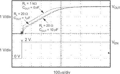
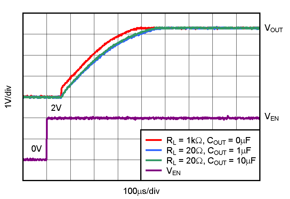
TPS732 TPS73233 Turn-On Response
Legacy silicon 
Figure 7-3 TPS73233 Turn-On Response
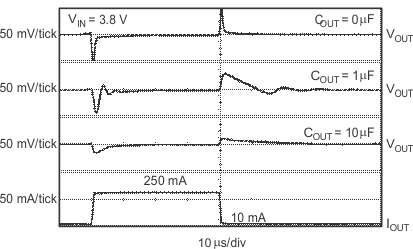
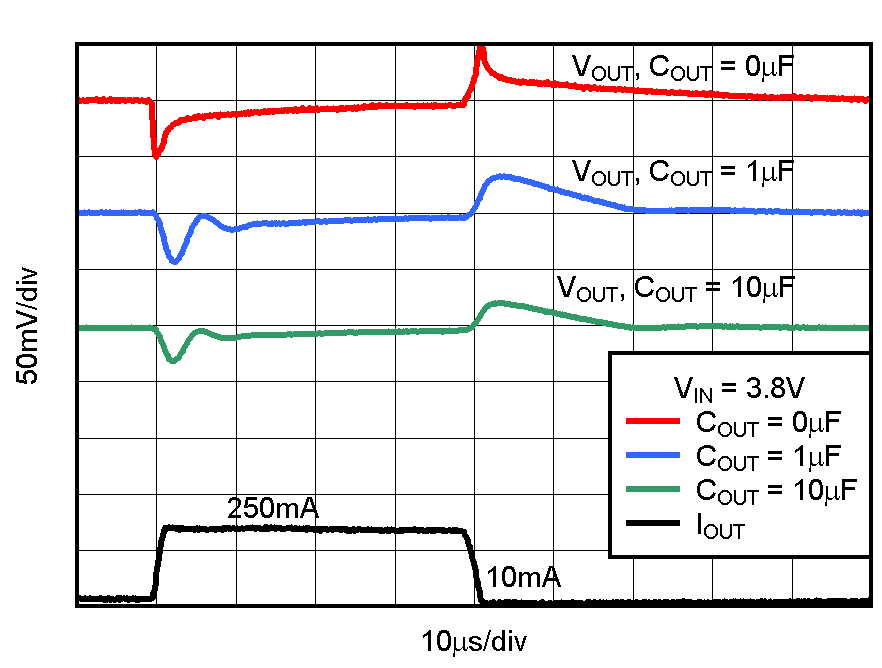
TPS732 TPS73233 Load Transient Response
Legacy silicon 
Figure 7-5 TPS73233 Load Transient Response
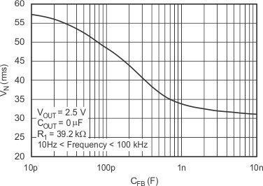
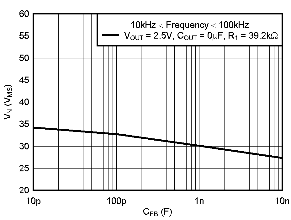
TPS732 TPS73201 RMS Noise Voltage vs CFB
Legacy silicon 
Figure 7-7 TPS73201 RMS Noise Voltage vs CFB
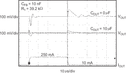
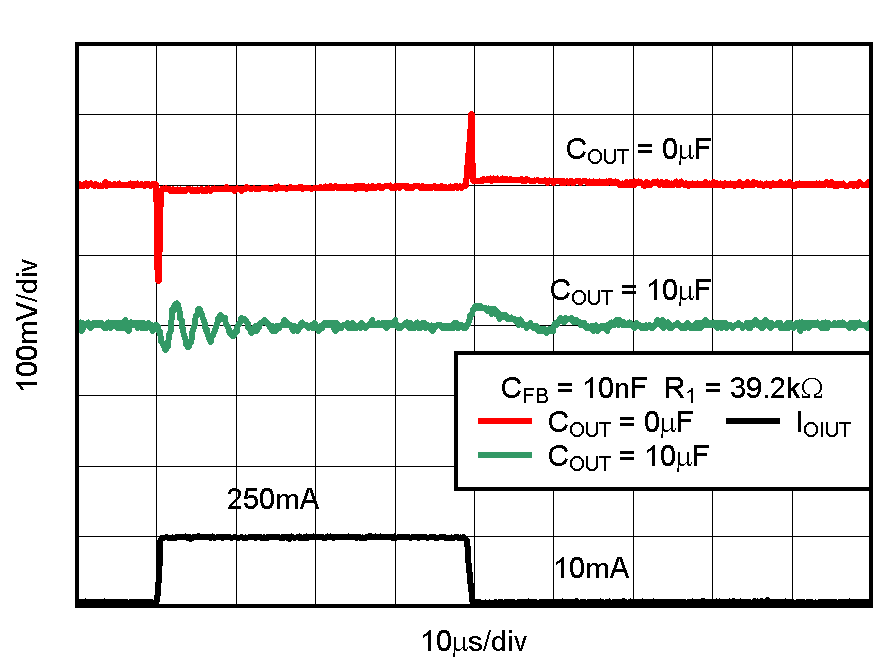
TPS732 TPS73201 Load Transient, Adjustable Version
Legacy silicon 
Figure 7-9 TPS73201 Load Transient, Adjustable Version
TPS732 TPS73233 Turn-On Response
New silicon, M3 suffix 
Figure 7-4 TPS73233 Turn-On Response
TPS732 TPS73233 Load Transient Response
New silicon, M3 suffix 
Figure 7-6 TPS73233 Load Transient Response
TPS732 TPS73201 RMS Noise Voltage vs CFB
New silicon, M3 suffix 
Figure 7-8 TPS73201 RMS Noise Voltage vs CFB
TPS732 TPS73201 Load Transient, Adjustable Version
New silicon, M3 suffix 
Figure 7-10 TPS73201 Load Transient, Adjustable Version