ZHCSW86F July   2005  – August 2024 LMH6702QML-SP

PRODUCTION DATA  

  1.   1
  2. 1特性
  3. 2应用
  4. 3说明
  5. 4Pin Configuration and Functions
  6. 5Specifications
    1. 5.1 Absolute Maximum Ratings
    2. 5.2 Recommended Operating Conditions
    3. 5.3 Quality Conformance Inspection
    4. 5.4 Electrical Characteristics: DC Parameters
    5. 5.5 Electrical Characteristics: AC Parameters
    6. 5.6 Electrical Characteristics: Drift Values Parameters
    7. 5.7 Typical Characteristics
  7. 6Application and Implementation
    1. 6.1 Application Information
      1. 6.1.1 Feedback Resistor
      2. 6.1.2 Harmonic Distortion
      3. 6.1.3 Capacitive Load Drive
      4. 6.1.4 DC Accuracy and Noise
    2. 6.2 Layout
      1. 6.2.1 Layout Guidelines
  8. 7Device and Documentation Support
    1. 7.1 接收文档更新通知
    2. 7.2 支持资源
    3. 7.3 Trademarks
    4. 7.4 静电放电警告
    5. 7.5 术语表
  9. 8Revision History
  10. 9Mechanical, Packaging, and Orderable Information

Feedback Resistor

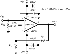
LMH6702QML-SP Recommended Noninverting Gain
                    Circuit Figure 6-1 Recommended Noninverting Gain Circuit
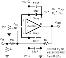
LMH6702QML-SP Recommended Inverting Gain
                    Circuit Figure 6-2 Recommended Inverting Gain Circuit

The LMH6702 achieves excellent pulse and distortion performance by using current feedback topology. The loop gain for a current-feedback op amp, and thus the frequency response, is predominantly set by the feedback-resistor value. The LMH6702 is optimized for use with a 237Ω feedback resistor. Using lower values can lead to excessive ringing in the pulse response while a higher value limits the bandwidth. Application Note OA-13 SNOA366 discusses this configuration in detail along with the occasions where a different RF can be advantageous.