ZHCSWR1H December 2009 – July 2024 DRV8412
PRODUCTION DATA
- 1
- 1特性
- 2应用
- 3说明
- 4Pin Configuration and Functions
- 5Specifications
- 6Detailed Description
-
Application and Implementation
- 7.1 Application Information
- 7.2 Typical Applications
- 7.3 Power Supply Recommendations
- 7.4 Layout
- 7Device and Documentation Support
- 8Revision History
- 9Mechanical, Packaging, and Orderable Information
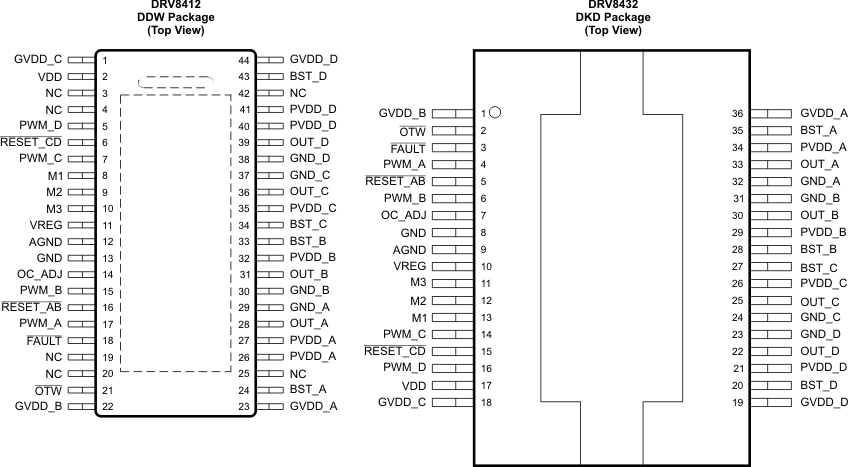
4 Pin Configuration and Functions

Table 4-1 Pin Functions
| PIN | I/O TYPE (1) | DESCRIPTION | ||
|---|---|---|---|---|
| NAME | DRV8412 | DRV8432 | ||
| AGND | 12 | 9 | P | Analog ground |
| BST_A | 24 | 35 | P | High side bootstrap supply (BST), external capacitor to OUT_A required |
| BST_B | 33 | 28 | P | High side bootstrap supply (BST), external capacitor to OUT_B required |
| BST_C | 34 | 27 | P | High side bootstrap supply (BST), external capacitor to OUT_C required |
| BST_D | 43 | 20 | P | High side bootstrap supply (BST), external capacitor to OUT_D required |
| GND | 13 | 8 | P | Ground |
| GND_A | 29 | 32 | P | Power ground for half-bridge A |
| GND_B | 30 | 31 | P | Power ground for half-bridge B |
| GND_C | 37 | 24 | P | Power ground for half-bridge C |
| GND_D | 38 | 23 | P | Power ground for half-bridge D |
| GVDD_A | 23 | 36 | P | Gate-drive voltage supply |
| GVDD_B | 22 | 1 | P | Gate-drive voltage supply |
| GVDD_C | 1 | 18 | P | Gate-drive voltage supply |
| GVDD_D | 44 | 19 | P | Gate-drive voltage supply |
| M1 | 8 | 13 | I | Mode selection pin |
| M2 | 9 | 12 | I | Mode selection pin |
| M3 | 10 | 11 | I | Reserved mode selection pin, AGND connection is recommended |
| NC | 3, 4, 19, 20, 25, 42 | — | — | No connection pin. Ground connection is recommended |
| OC_ADJ | 14 | 7 | O | Analog overcurrent programming pin, requires resistor to AGND |
| OTW | 21 | 2 | O | Overtemperature warning signal, open-drain, active-low. An internal pullup resistor to VREG (3.3 V) is provided on output. Level compliance for 5-V logic can be obtained by adding external pullup resistor to 5 V |
| OUT_A | 28 | 33 | O | Output, half-bridge A |
| OUT_B | 31 | 30 | O | Output, half-bridge B |
| OUT_C | 36 | 25 | O | Output, half-bridge C |
| OUT_D | 39 | 22 | O | Output, half-bridge D |
| PVDD_A | 26, 27 | 34 | P | Power supply input for half-bridge A requires close decoupling capacitor to ground. |
| PVDD_B | 32 | 29 | P | Power supply input for half-bridge B requires close decoupling capacitor to gound. |
| PVDD_C | 35 | 26 | P | Power supply input for half-bridge C requires close decoupling capacitor to ground. |
| PVDD_D | 40, 41 | 21 | P | Power supply input for half-bridge D requires close decoupling capacitor to ground. |
| PWM_A | 17 | 4 | I | Input signal for half-bridge A |
| PWM_B | 15 | 6 | I | Input signal for half-bridge B |
| PWM_C | 7 | 14 | I | Input signal for half-bridge C |
| PWM_D | 5 | 16 | I | Input signal for half-bridge D |
| RESET_AB | 16 | 5 | I | Reset signal for half-bridge A and half-bridge B, active-low |
| RESET_CD | 6 | 15 | I | Reset signal for half-bridge C and half-bridge D, active-low |
| FAULT | 18 | 3 | O | Fault signal, open-drain, active-low. An internal pullup resistor to VREG (3.3 V) is provided on output. Level compliance for 5-V logic can be obtained by adding external pullup resistor to 5 V |
| VDD | 2 | 17 | P | Power supply for digital voltage regulator requires capacitor to ground for decoupling. |
| VREG | 11 | 10 | P | Digital regulator supply filter pin requires 0.1-μF capacitor to AGND. |
| THERMAL PAD | — | N/A | T | Solder the exposed thermal pad to the landing pad on the pcb. Connect landing pad to bottom side of pcb through via for better thermal dissipation. This pad should be connected to GND. |
| HEAT SLUG | N/A | — | T | Mount heat sink with thermal interface on top of the heat slug for best thermal performance. |
(1) I = input, O = output, P = power, T = thermal
Table 4-2 Mode Selection Pins
| MODE PINS | OUTPUT CONFIGURATION | DESCRIPTION | ||
|---|---|---|---|---|
| M3 | M2 | M1 | ||
| 0 | 0 | 0 | 2 FB or 4 HB | Dual full bridges (two PWM inputs each full bridge) or four half bridges with cycle-by-cycle current limit |
| 0 | 0 | 1 | 2 FB or 4 HB | Dual full bridges (two PWM inputs each full bridge) or four half bridges with OC latching shutdown (no cycle-by-cycle current limit) |
| 0 | 1 | 0 | 1 PFB | Parallel full bridge with cycle-by-cycle current limit |
| 0 | 1 | 1 | 2 FB | Dual full bridges (one PWM input each full bridge with complementary PWM on second half bridge) with cycle-by-cycle current limit |
| 1 | x | x | Reserved | |