ZHCU710 October   2019


  1.    说明
  2.    资源
  3.    特性
  4.    应用
  5.    设计图像
  6. 1System Description
    1. 1.1 Key System Specifications
  7. 2System Overview
    1. 2.1 Block Diagram
    2. 2.2 Design Considerations
    3. 2.3 Highlighted Products
      1. 2.3.1 TLV61048
      2. 2.3.2 TPS560430
      3. 2.3.3 TL431
      4. 2.3.4 CSD25310Q2
    4. 2.4 System Design Theory
      1. 2.4.1 Super Capacitor Linear Charger Circuit
      2. 2.4.2 Boost Converter Solution
      3. 2.4.3 Buck Converter Solution
  8. 3Hardware, Software, Testing Requirements, and Test Results
    1. 3.1 Required Hardware and Software
      1. 3.1.1 Hardware
    2. 3.2 Testing and Results
      1. 3.2.1 Test Setup
      2. 3.2.2 Test Results
        1. 3.2.2.1 Linear Charger Operating Waveform
        2. 3.2.2.2 Transient Waveform When Vbus fails
        3. 3.2.2.3 Super Capacitor Discharging Waveform
  9. 4Design Files
    1. 4.1 Schematics
    2. 4.2 Bill of Materials
    3. 4.3 PCB Layout Recommendations
      1. 4.3.1 Layout Prints
    4. 4.4 Altium Project
    5. 4.5 Gerber Files
    6. 4.6 Assembly Drawings
  10. 5Software Files
  11. 6Related Documentation
    1. 6.1 商标
    2. 6.2 Third-Party Products Disclaimer

Block Diagram

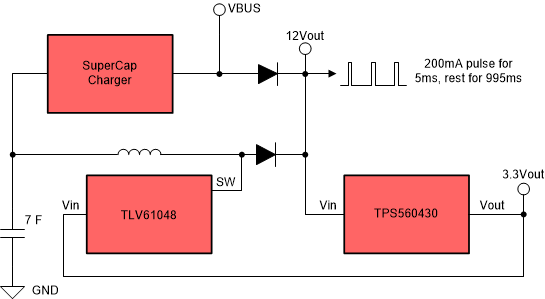
Figure 1 shows the block diagram of TIDA-050033. It uses a super capacitor as the energy storage cell. When VBUS exists, the PLC module is powered by Vbus and the super capacitor is charged by a linear charger. The super capacitor will be charged to 2.5 V. The synchronous step-down DC-DC converter TPS560430 will generate a 3.3 V dc voltage as MCU power supply and TLV61048 external bias. When Vbus fails (Vbus < 12 V), boost converter TLV61048 starts switching and provides a 12 V seamlessly to supply the PLC line driver amplifier

Figure 1. TIDA-050033 Block DiagramTIDA-050033 SystemBlockDiagram.gif