ZHCU710 October   2019


  1.    说明
  2.    资源
  3.    特性
  4.    应用
  5.    设计图像
  6. 1System Description
    1. 1.1 Key System Specifications
  7. 2System Overview
    1. 2.1 Block Diagram
    2. 2.2 Design Considerations
    3. 2.3 Highlighted Products
      1. 2.3.1 TLV61048
      2. 2.3.2 TPS560430
      3. 2.3.3 TL431
      4. 2.3.4 CSD25310Q2
    4. 2.4 System Design Theory
      1. 2.4.1 Super Capacitor Linear Charger Circuit
      2. 2.4.2 Boost Converter Solution
      3. 2.4.3 Buck Converter Solution
  8. 3Hardware, Software, Testing Requirements, and Test Results
    1. 3.1 Required Hardware and Software
      1. 3.1.1 Hardware
    2. 3.2 Testing and Results
      1. 3.2.1 Test Setup
      2. 3.2.2 Test Results
        1. 3.2.2.1 Linear Charger Operating Waveform
        2. 3.2.2.2 Transient Waveform When Vbus fails
        3. 3.2.2.3 Super Capacitor Discharging Waveform
  9. 4Design Files
    1. 4.1 Schematics
    2. 4.2 Bill of Materials
    3. 4.3 PCB Layout Recommendations
      1. 4.3.1 Layout Prints
    4. 4.4 Altium Project
    5. 4.5 Gerber Files
    6. 4.6 Assembly Drawings
  10. 5Software Files
  11. 6Related Documentation
    1. 6.1 商标
    2. 6.2 Third-Party Products Disclaimer

Buck Converter Solution

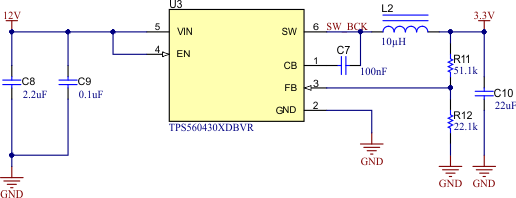
Figure 4 shows the TPS560430 buck converter. TPS560430 operates at 1.1 MHz switching frequency for high efficiency. It provides 3.3 V to supply MCU and boost converter TLV61048 VIN pin. At light load condition, the TPS560430 operates in PFM mode to maintain high efficiency. When Vbus fails, TLV61048 boost output supplies the PLC line driver, as well as the buck input

Figure 4. TPS560430 Buck ConverterTIDA-050033 TPS560430BuckConverter.gif