ZHCU710 October   2019


  1.    说明
  2.    资源
  3.    特性
  4.    应用
  5.    设计图像
  6. 1System Description
    1. 1.1 Key System Specifications
  7. 2System Overview
    1. 2.1 Block Diagram
    2. 2.2 Design Considerations
    3. 2.3 Highlighted Products
      1. 2.3.1 TLV61048
      2. 2.3.2 TPS560430
      3. 2.3.3 TL431
      4. 2.3.4 CSD25310Q2
    4. 2.4 System Design Theory
      1. 2.4.1 Super Capacitor Linear Charger Circuit
      2. 2.4.2 Boost Converter Solution
      3. 2.4.3 Buck Converter Solution
  8. 3Hardware, Software, Testing Requirements, and Test Results
    1. 3.1 Required Hardware and Software
      1. 3.1.1 Hardware
    2. 3.2 Testing and Results
      1. 3.2.1 Test Setup
      2. 3.2.2 Test Results
        1. 3.2.2.1 Linear Charger Operating Waveform
        2. 3.2.2.2 Transient Waveform When Vbus fails
        3. 3.2.2.3 Super Capacitor Discharging Waveform
  9. 4Design Files
    1. 4.1 Schematics
    2. 4.2 Bill of Materials
    3. 4.3 PCB Layout Recommendations
      1. 4.3.1 Layout Prints
    4. 4.4 Altium Project
    5. 4.5 Gerber Files
    6. 4.6 Assembly Drawings
  10. 5Software Files
  11. 6Related Documentation
    1. 6.1 商标
    2. 6.2 Third-Party Products Disclaimer

Super Capacitor Discharging Waveform

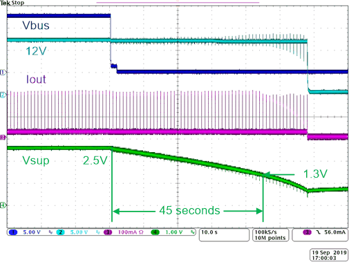
Figure 7 shows the super capacitor discharging waveform. When Vbus fails, the super capacitor takes the role of backup power source. Boost converter TLV61048 draws power from super capacitor and supply the PLC module. The test result shows TLV61048 could provide stable 12 V/ 200 mA even super capacitor voltage decreases to 1.3 V. The discharging time lasts 45 seconds. It maximizes the super capacitor usage rate.

Figure 7. Super Capacitor Discharging WaveformTIDA-050033 7SuperCapDischarging.gif