ZHCU734A January 2017 – March 2020
3.1 Hardware and Resources Guide
Figure 13 shows some of the key components on the actual hardware.
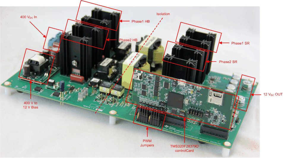 Figure 13. TIDM-1001 – Two-Phase Interleaved LLC Resonant Converter Board
 Table 2 shows the key signal connections between the TMS320F280025C controlCARD and the TIDM-1001 base board. For reference relevant portions of the schematic are also provided in Figure 14 to Figure 18.
Table 2. Key Signal Connections
This design uses a lot of jumper options for experimentation but there are some jumpers that must be populated for proper operation of the board. The jumpers that must be populated are listed below:
- J6
- J7
- J8
- J14 (positions 1 to 2, 3 to 4, 5 to 6, 7 to 8, 11 to 12, 13 to 14, 15 to 16, 17 to 18)
- J15 (for stand-alone or DEMO operation)
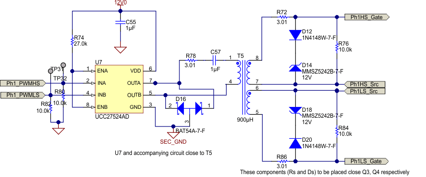
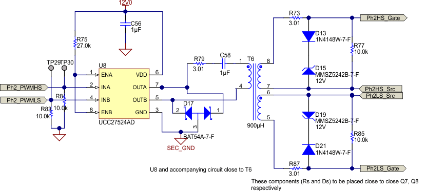 Figure 14. TIDM-1001 – HB PWM Drive Circuit
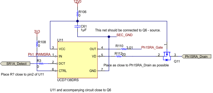
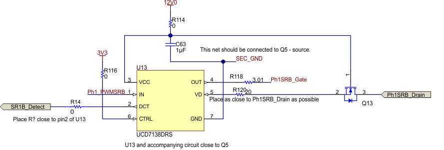 Figure 15. TIDM-1001 – Phase-One SR PWM Driver Circuit
 Figure 16. TIDM-1001 – Phase-Two SR PWM Driver Circuit
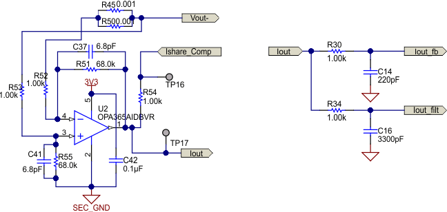
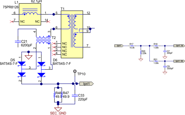 Figure 17. TIDM-1001 – Iout and Ipri1 Feedback Circuit
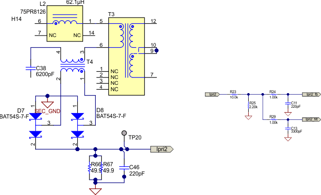
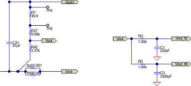 Figure 18. TIDM-1001 – Ipri2 and Vout Feedback Circuit