ZHCU741 July 2020
- 说明
- 资源
- 特性
- 应用
- 5
- 1System Description
- 2System Overview
-
3Hardware, Software, Testing Requirements, and Test Results
- 3.1 Hardware Requirements
- 3.2 Test Setup
- 3.3
Test Results
- 3.3.1 Boost Turn on Delay
- 3.3.2 Highbeam/Lowbeam Turn on Delay
- 3.3.3 Highbeam/Lowbeam Switch Node and Ripple Current
- 3.3.4 Turn Indicator Turn on Delay
- 3.3.5 Turn Indictor Turn Off Delay
- 3.3.6 Turn Indicator 1.5 Hz Operation
- 3.3.7 Turn Indicator Output Voltage and Current
- 3.3.8 Daytime Running Light Turn-on Delay
- 3.3.9 Daytime Running Light Switch Node and Output Current
- 3.3.10 Highbeam/Lowbeam LED Short
- 3.3.11 Highbeam/Lowbeam Fault Indicator
- 3.3.12 Turn Indicator Fault Output
- 3.3.13 TPS92682-Q1 Boost and SEPIC Interleaving
- 3.3.14 TIDA-050040 Full Load Efficiency
- 3.3.15 Efficiency Highbeam/Lowbeam
- 3.3.16 Efficiency Turn Indicator and Daytime Running Light
- 3.3.17 Efficiency Highbeam/Lowbeam and Turn Indicator
- 3.3.18 CISPR 25 Class 5 EMI Scan
- 3.3.19 Top Side Thermal Image DRL at 15W
- 3.3.20 Bottom side thermal image DRL at 15W
- 3.3.21 Top Side Thermal Image Highbeam/Lowbeam at 30W, Turn Indicator at 7.5W average
- 3.3.22 Bottom Side Thermal Image Highbeam/Lowbeam at 30W, Turn Indicator at 7.5W average
- 4Design and Documentation Support
2.3.3 TPS92520-Q1
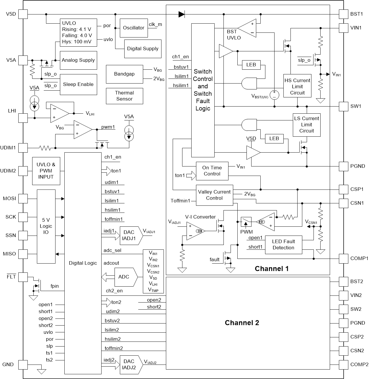
The TPS92520-Q1 is a monolithic dual synchronous buck LED driver with a wide 4.5-V to 65-V operating input voltage range that can independently power two strings of series connected LEDs. The TPS92520-Q1 implements an adaptive on-time average current mode control and is designed to be compatible with shunt FET dimming techniques and LED matrix manager based dynamic beam headlamps. The adaptive on-time control provides near constant switching frequency that can be set between 100-kHz and 2.2-MHz. Inductor current sensing and closed loop feedback enables better than ±4% accuracy over wide input voltage, output voltage and ambient temperature range.
The high performance LED driver can independently modulate LED current using both analog or PWM dimming techniques. Linear analog dimming response with over 16:1 range is obtained by programming the 10-bit IADJ value via SPI. PWM dimming of LED current is achieved by directly modulating the corresponding UDIM input pin with the desired duty cycle or by enabling the internal PWM generator circuit. The PWM generator translates the 10-bit PWM register value to a corresponding duty cycle by comparing it to a programmable digital counter.
The TPS92520-Q1 incorporates advanced SPI programmable diagnostic and fault protection featuring: cycle-by-cycle switch current limit, bootstrap undervoltage, LED open, LED short, thermal warning and thermal shutdown. An on-board 10-bit ADC samples critical input parameters required for system health monitoring and diagnostics.
(The TPS92520-Q1 is available in a 8.1-mm x 11-mm thermally-enhanced 32-pin HTSSOP package with a 2.75-mm x 3.45-mm top-exposed and bottomexposed pad.)
 Figure 2-3 TPS92520-Q1 Functional Block
Diagram