ZHCU759 July 2021
- 说明
- 资源
- 特性
- 应用
- 5
- 1System Description
-
2System Overview
- 2.1 Block Diagram
- 2.2
Design Considerations
- 2.2.1 System Control and Processing
- 2.2.2 Analog Front End
- 2.2.3 Input Voltage Monitoring: 5 V, 20 V, 40 V, and ±5 V
- 2.2.4 Bidirectional Current Sense: ±2 A
- 2.2.5 Unipolar Current Sense: 0.25 A to 1 A
- 2.2.6 TMP461-SP: Local and Remote Temperature Sensing
- 2.2.7 NTC Thermistor Temperature Sensing
- 2.2.8 Adjustable Voltage Source
- 2.2.9 Fixed Output Current Source
- 2.2.10 Adjustable 4-mA Current Source
- 2.2.11 Power Tree and Power Sequencing
- 2.3 Highlighted Products
- 3Hardware, Software, Testing Requirements, and Test Results
- 4Design and Documentation Support
- 5About the Author
3.1.2 Software
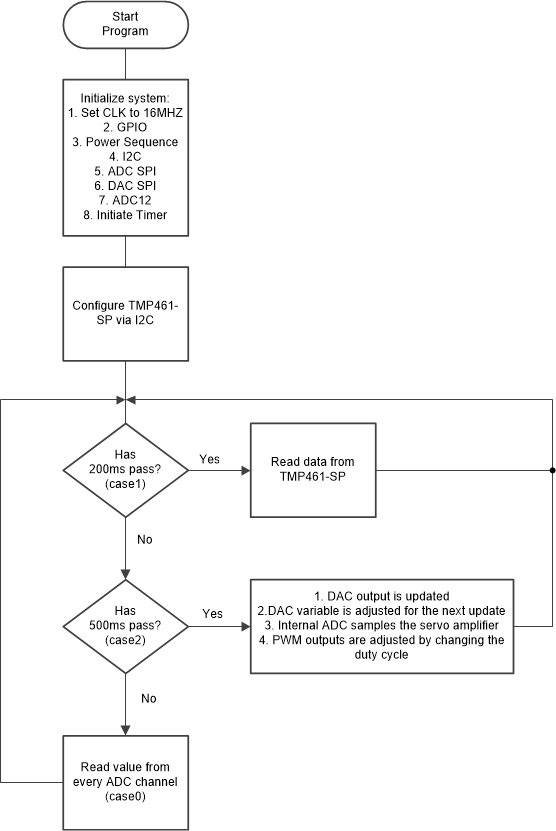
Solution-specific and device-independent files are provided as .c/.h files. The main.c file provides the initialization of the GPIOs, I2C and SPI communication, ADC or DAC setup, PWM setup for the nonsynchronous boost, and power sequencing. The software is required to power up the board properly as well as read the ADC data.
To program the MSP430FR5969-SP independently, make sure no other jumpers are installed and provide an external 3.3 V to J16 (for the external ADC circuit) and J36 (for the integrated ADC solution). This only powers on the MSP430FR5969-SP so that adjustments to the power sequencing are done without damaging the ADC128S102QML-SP.
In main.c the variable "ext_int" is set to either 0 or 1 to run two different functions. When "ext_int" is set to 0, it runs the code to read all the channels from the external ADC via SPI. If "ext_int" is set to 1, the code reads all inputs from the integrated ADC. The ADC reads are done via low power interrupts to save on processing power of the MSP430. The values are then stored in the FRAM and are accessed when the software is paused. Each ADC channel corresponds to a specific point in memory with a memory word length default of 1000 and can be changed via the variable WRITE_SIZE.
 Figure 3-1 Software Flow
To access the data in FRAM from Code Composer Studio (CCS), open the memory browser (View → Memory Browser) and type the starting address outlined in Table 3-1 and Table 3-2. Select save memory and save it as a .dat file (this file type can be opened with Microsoft® Excel®). The save memory function allows saving of the data in different formats for different processing requirements. After selecting the file location to save the file, enter the start address and specify the length of the array (default is 1000). Opening the .dat file shows the raw ADC data in column one. To convert the integer values, use the ADC equation (Equation 5) in a column next to the data captured to convert the integer values to voltage, where n is the number of bits used for the measurement.
| ADC BUFFER | ADC128S102-SP ADC CHANNEL | MEASURED RAIL | MEMORY LOCATION |
|---|---|---|---|
|
adc_buffer_0 |
IN0 |
500 µA |
x004400 |
| adc_buffer_1 |
IN1 |
±2 A |
x0047E8 |
| adc_buffer_2 |
IN2 |
20 V |
x004BD0 |
| adc_buffer_3 |
IN3 |
Temperature voltage |
x004FB8 |
| adc_buffer_4 |
IN4 |
±5 V |
x0053A0 |
| adc_buffer_5 |
IN5 |
40 V |
x005788 |
| adc_buffer_6 |
IN6 |
0.25 A–1 A |
x005B70 |
| adc_buffer_7 |
IN7 |
5 V |
x005F58 |
| ADC BUFFER | MSP430 ADC12 CHANNEL | MEASURED RAIL | MEMORY LOCATION |
|---|---|---|---|
|
adc_buffer_0 |
A0 |
500 µA |
x004400 |
| adc_buffer_1 |
A8 |
40 V |
x0047E8 |
| adc_buffer_2 |
A9 |
0.25 A–1 A |
x004BD0 |
| adc_buffer_3 |
A10 |
5 V |
x004FB8 |
| adc_buffer_4 |
A12 |
±2 A |
x0053A0 |
| adc_buffer_5 |
A13 |
20 V |
x005788 |
| adc_buffer_6 |
A14 |
Temperature voltage |
x005B70 |
| adc_buffer_7 |
A15 |
±5 V |
x005F58 |