ZHCU772 December 2021
- 说明
- 资源
- 特性
- 应用
- 5
- 1System Overview
- 2Hardware, Software, Testing Requirements, and Test Results
- 3Design and Documentation Support
- 4About the Author
- 5Acknowledgement
2.1.1.1 Clocking Board Setup
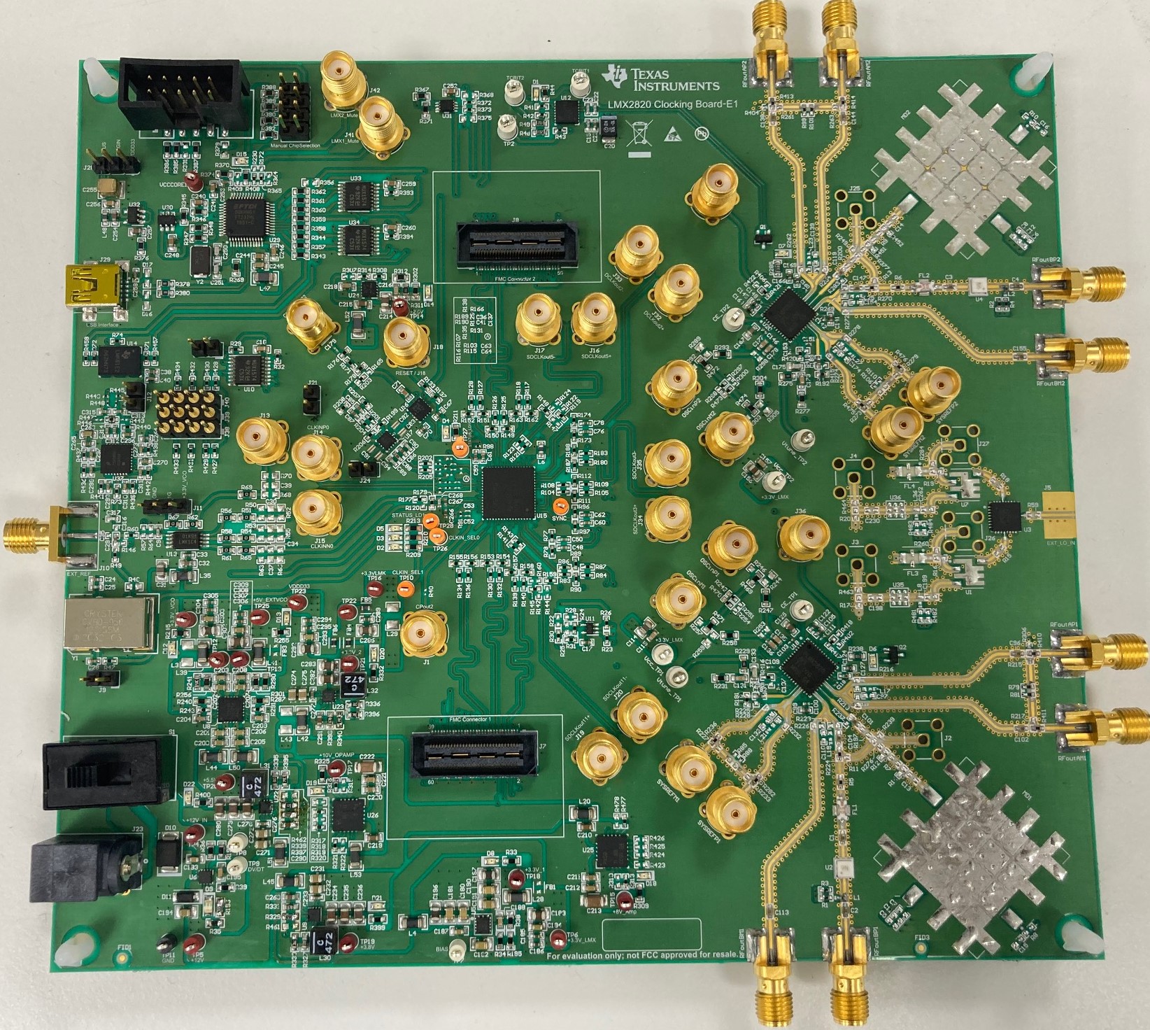
Figure 2-1 shows the multichannel LMX2820 clocking board.
 Figure 2-1 Multichannel Clocking
Board
Figure 2-1 Multichannel Clocking
BoardReference the following for clocking board setup:
- Power Supply
Power supply connector J23: This connector is used to connect the power supply. Set the power supply to 12 V with a 3-A current limit.
- Input reference signals
- Option 1: Connect the external reference signal to EXT_REF connector (J10). While connecting the external reference, disconnect the Y1 and U14/U37 connection by removing C29 and C316, and place C35. Disconnect the power supply of Y1 and U14 by removing jumpers J9 and J12. For reference enable to the clocking devices from the reference buffer device U13, place the short jumper at pin 2-3 of jumper J11.
- Option 2: The onboard reference LMK61E2 (U14) is powered up using the jumper J12 and factory programmed to generate a 156-MHz LVDS output. U14 can be programmed to generate different clock frequencies using the I2C interface. LVDS output is translated to LVCMOS format using U37 and output enabled by shorting pin 1 of the jumpers J39-J40. While using the onboard LMK61E2, disconnect the clock inputs from Y1 and external reference by removing C29 and C35, then place C316. Isolate the power supply to Y1 by removing J9. For reference enable to clocking devices from reference buffer device U13, place the short jumper at pin 2-3 of jumper J11.
- Option 3: The onboard VCXO Y1 is powered on using the jumper J9 and outputs a 122.88-MHz signal to the LMK04832 OSCin_P pin input. In this option, LMX2820 devices receive the reference signals from the LMK04832 DCLK ports. While using Y1, disconnect the clock inputs from LMK61E2 (U14) and external reference by removing C316, C35, C29, and R177, and place the R146 and R120. At the same time, isolate the power supply to U14 by removing the jumper J12.
- Option 4: Use one of the previous options, when LMK04832 works in PLL mode. When LMK04832 is operating in distribution mode, connect the external reference to external connector J18 or J22 based on operating input frequency. While operating in distribution mode, power down the Y1 and U14 by removing jumpers J9 and J12.
- Input sync signal
Connect the external sync signal at external J14 and J15 connectors to reset the LMK04832 dividers.
- Output signals
- LMX2820 amplified outputs are generated at RFoutBP1 and RFoutBP2 connectors as DCLK and are connected to AFE7950EVMs as an external sampling clock.
- SYSREFM1 and SYSREFM2 connectors generate the low-frequency SYSREF signals for AFE7950EVM.
- Connectors J7 and J8 generate the FPGA CLKs and SYSREFs for two TSW14J56 capture cards.
- Programming interface
Connect the USB mini cable to the onboard USB connector J29 and test the PC to program the LMX2820 clocking board devices using the clocking board software GUI.