ZHCU772 December 2021
- 说明
- 资源
- 特性
- 应用
- 5
- 1System Overview
- 2Hardware, Software, Testing Requirements, and Test Results
- 3Design and Documentation Support
- 4About the Author
- 5Acknowledgement
1.4.1.2 JESD204B-Compliant Multichannel Phase Synchronized Clocks Generation
The latest RF sampling data converter supports a JESD204B-compliant interface, which needs a high-frequency sampling clock and system reference signal called SYSREF. When clocking multiple RF transceivers, channel-to-channel skew becomes an important design consideration. Clock jitter and phase mismatch leads to deviation from the ideal sampling instant of a channel and thereby, results in channel-to-channel skew. To achieve the excellent phase noise performance at high frequencies, LMX2820 synthesizers used in this reference design, which brings down the clock jitter to around 45 fs.
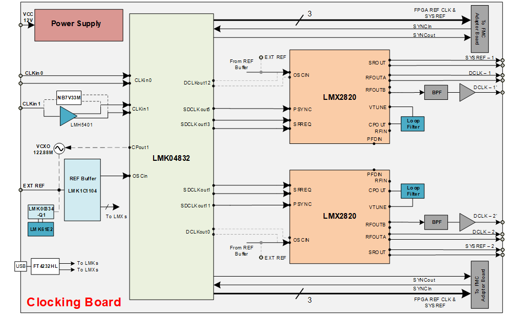
Figure 1-3 shows the block diagram of a multichannel JESD204B-compliant clocking board. A common reference frequency can be fed externally, or generated by onboard VCXO or LMK61E2 and is provided to the LMK04832 at the OSCin input through the reference buffer LMK1C1104. The LMK04832 on this design is used to provide an FPGA reference clock and SYSREF to the TSW14J56EVM capture card through the FMC adapter board and SYSREF to AFE7950EVMs through LMX2820 in repeater mode. The LMK04832 is configured in PLL mode to phase synchronize OSCin and the remaining generated clocks.
To generate the phase-synchronized device clocks to AFE7950EVMs, a common reference frequency is input to the OSCin of the two LMX2820 synthesizers using LMK1C1104 and the SYNC signals from LMK04832. As Figure 1-3 shows, SYSREF and the device clock to the AFE7950EVMs are provided through LMX2820, where SYSREF is distributed in repeater mode. For multi-device JESD204B synchronization, device clocks should be phase aligned and meet the SYSREF setup and hold time of the AFE7950 device.
 Figure 1-3 Clocking Board Block
Diagram
Figure 1-3 Clocking Board Block
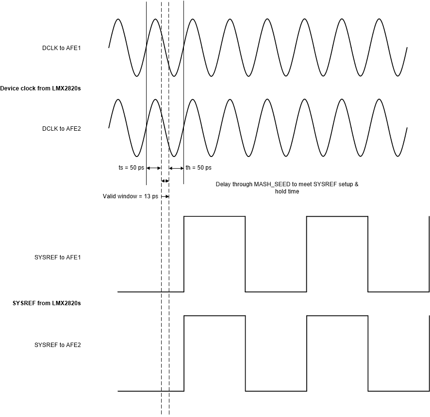
DiagramFigure 1-4 shows the waveform of the device clocks and SYSREF to both AFE7950EVMs. In this design, the device clock of the AFE7950 is 8847.36 MHz and SYSREF setup and hold time of the AFE7950 are 50 ps each. With this, the valid window for meeting the setup and hold time is approximately 13 ps, which is less than the step size (25 ps) of SYSREF from the LMK04832. Hence, phase delay must be provided in device clocks, which is done by the MASH_SEED value in the LMX2820 as well as SYSREF phase delay in the steps of 9 ps from LMX2820. Each LMX2820 device may require tuning for the MASH_SEED delays to achieve in-phase generated clocks and meet the setup and hold time of the SYSREFs.
 Figure 1-4 Clock Timing Waveforms
Reference frequency to the clocking board can be any standard frequency such as 10 MHz, 100 MHz, and so forth as per the operating clock frequency. In this design, the AFE7950 performance and synchronization test performed at 8847.36 MHz on the device clock is done to show the comparison with the internal PLL clock mode. To generate the synchronized device clock, the LMX2820 operates in integer PLL mode along with SYNC enable. The LMX2820 can operate at higher reference frequency along with phase detector frequency for better phase noise performance. In this design, an external input reference frequency of 184.32 MHz is provided to the LMX2820 devices by the sig gen through reference buffer LMK1C1104. The phase-detector frequency also changes to 184.32 MHz, and the loop filter configuration is the same as the LMX2820EVM.
Table 1-2 details the loop filter component values.
| Parameter | Value |
|---|---|
| C1_LF | 470 pF |
| C2_LF | 68 nF |
| C3_L3 | 2.2 nF |
| R2_LF | 68.1 Ω |
| R3_LF | 18.2 Ω |