ZHCU772 December   2021


  1.   说明
  2.   资源
  3.   特性
  4.   应用
  5.   5
  6. 1System Overview
    1. 1.1 Key System Level Specifications
    2. 1.2 System Description
    3. 1.3 Block Diagram
    4. 1.4 Design Considerations
      1. 1.4.1 Frequency Band and Applications
        1. 1.4.1.1 RF Transceiver Synchronization Challenges
        2. 1.4.1.2 JESD204B-Compliant Multichannel Phase Synchronized Clocks Generation
      2. 1.4.2 Clock Jitter and System SNR
      3. 1.4.3 Power-Supply Selection
      4. 1.4.4 Highlighted Products
        1. 1.4.4.1 AFE7950
        2. 1.4.4.2 LMX2820
        3. 1.4.4.3 LMK04832
        4. 1.4.4.4 TPS62913 and TPS62912
        5. 1.4.4.5 LMK1C1104
  7. 2Hardware, Software, Testing Requirements, and Test Results
    1. 2.1 Required Hardware and Software
      1. 2.1.1 Hardware
        1. 2.1.1.1 Clocking Board Setup
        2. 2.1.1.2 FMC-to-FMC Adapter Board Setup
        3. 2.1.1.3 AFE7950EVM Setup
        4. 2.1.1.4 TSW14J56EVM Setup
        5. 2.1.1.5 Hardware Setup of Multiple Transceiver Synchronization
      2. 2.1.2 Software
        1. 2.1.2.1 TIDA-010230 Clocking Board GUI
        2. 2.1.2.2 AFE7950 EVM GUI
        3. 2.1.2.3 High-Speed Data Converter (HSDC) Pro
        4. 2.1.2.4 Programming Steps
        5. 2.1.2.5 Clocking Board Programming Sequence
        6. 2.1.2.6 Latte SW and HSDC Pro Setup
    2. 2.2 Test Setup
    3. 2.3 Test Results
      1. 2.3.1 LMX2820 Phase-Noise Performance
      2. 2.3.2 AFE7950 Transmitter Performance
      3. 2.3.3 AFE7950 Receiver Performance
      4. 2.3.4 Multiple AFE7950s TX and RX Alignment
      5. 2.3.5 Summary and Conclusion
  8. 3Design and Documentation Support
    1. 3.1 Design Files
      1. 3.1.1 Schematics
      2. 3.1.2 BOM
    2. 3.2 Tools and Software
    3. 3.3 Documentation Support
    4. 3.4 支持资源
    5. 3.5 Trademarks
  9. 4About the Author
  10. 5Acknowledgement

Clocking Board Programming Sequence

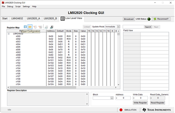
All devices in the clocking board are configured by loading the configuration files in the low-level view page.

  1. Load the LMK04832_2949.12M_184.32MREF_SYSREF_SYNC.cfg file to program onboard LMK04832 to generate FPGA REF clock and SYSREFs
  2. Load the LMX2820_A_B_8847.36M_184.32MREF_SYSREF_REPT_SYNC.cfg file to generate synchronized device clocks at 8847.36 MHz and SYSREF in repeater mode from LMX2820s
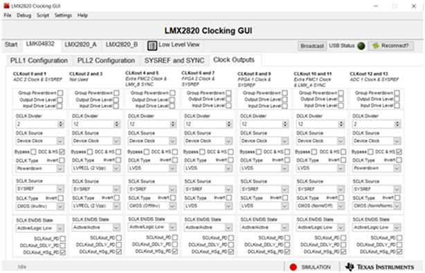
  3. Once all other boards are programmed, turn off the SYSREF to AFE7950EVM by setting Active/Logic Low for SDCLK1 and SDCLK13 from the clocking board
GUID-20211018-SS0I-PTJH-FMVL-FF5FWDNHR6Q0-low.png Figure 2-4 LMX2820 Clocking GUI
GUID-20211018-SS0I-R5TC-TQ3H-VQMHZ50SSSNX-low.png Figure 2-5 LMX2820 Clocking GUI With LMK04832 Tab