SLLSEI3A September 2013 – November 2015 SN65HVD265 , SN65HVD266 , SN65HVD267
PRODUCTION DATA.
- 1 Features
- 2 Applications
- 3 Description
- 4 Revision History
- 5 Device Comparison Table
- 6 Pin Configurations and Functions
- 7 Specifications
- 8 Parameter Measurement Information
- 9 Detailed Description
- 10Application and Implementation
- 11Power Supply Recommendations
- 12Layout
- 13Device and Documentation Support
- 14Mechanical, Packaging, and Orderable Information
Package Options
Mechanical Data (Package|Pins)
- D|8
Thermal pad, mechanical data (Package|Pins)
Orderable Information
1 Features
- Meets the Requirements of ISO11898-2
- Turbo CAN:
- Specified for 2-Mbps CAN FD (CAN with Flexible Data Rate)
- Short and Symmetrical Propagation Delay Times and Fast Loop Times for Enhanced Timing Margin
- Higher Data Rates in CAN Networks
- I/O Voltage Range Supports 3.3-V and 5-V MCUs
- Ideal Passive Behavior When Unpowered
- Bus and Logic Terminals are High Impedance (no load)
- Power-Up/Down With Glitch Free Operation On Bus
- Protection Features
- HBM ESD Protection Exceeds ±12 kV
- Bus Fault Protection –27 V to 40 V
- Undervoltage Protection on Supply Terminals
- Driver Dominant Time Out (TXD DTO)
- SN65HVD267: Receiver Dominant Time Out (RXD DTO)
- SN65HVD267: FAULT Output Terminal
- Thermal Shutdown Protection
- Characterized for –40°C to 125°C Operation
2 Applications
- 2-Mbps Operation in CAN with Flexible Data Rate Networks
- 1-Mbps Operation in Highly Loaded CAN Networks Down to 10-kbps Networks Using TXD DTO
- Industrial Automation, Control, Sensors and Drive Systems
- Building, Security and Climate Control Automation
- Telecom Base Station Status and Control
- SN65HVD267: Functional Safety With Redundant and Multi-topology CAN networks
- CAN Bus Standards Such as CANopen, DeviceNet, NMEA2000, ARNIC825, ISO11783, CANaerospace
3 Description
This CAN transceiver meets the ISO1189-2 High Speed CAN (Controller Area Network) physical layer standard. It is designed for data rates in excess of 2 Mpbs (megabits per second) for CAN FD (CAN with flexible data rate), greater than 1 Mbps for CAN in short networks, and enhanced timing margin and higher data rates in long and highly-loaded networks. The device provides many protection features to enhance device and CAN-network robustness. The SN65HVD267 adds additional features, allowing easy design of redundant and multi-topology networks with fault indication for higher levels of safety in the CAN system.
Device Information (1)
| PART NUMBER | PACKAGE | BODY SIZE |
|---|---|---|
| SN65HVD26xD | SOIC (8) | 4.90 mm × 3.91 mm |
- For all available packages, see the orderable addendum at the end of the data sheet.
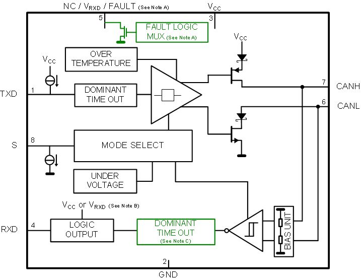
Functional Block Diagram

4 Revision History
Changes from * Revision (September 2013) to A Revision
- Added Pin Configuration and Functions section, ESD Ratings table, Switching Characteristics table, Feature Description section, Device Functional Modes, Application and Implementation section, Power Supply Recommendations section, Layout section, Device and Documentation Support section, and Mechanical, Packaging, and Orderable Information section Go
- Changed Typical Redundant Physical Layer Topology Using the SN65HVD267, Figure 19Go