-
ADC128S102QML-SP Radiation Hardened 8-Channel, 50 kSPS to 1 MSPS, 12-Bit A/D Converter
- 1 Features
- 2 Applications
- 3 Description
- 4 Revision History
- 5 Pin Configuration and Functions
-
6 Specifications
- 6.1 Absolute Maximum Ratings
- 6.2 ESD Ratings
- 6.3 Recommended Operating Conditions
- 6.4 Thermal Information
- 6.5 Electrical Characteristics: ADC128S102QML-SP Converter
- 6.6 Electrical Characteristics: Radiation
- 6.7 Electrical Characteristics: Burn in Delta Parameters - TA at 25°C
- 6.8 Timing Requirements
- 6.9 Typical Characteristics
- 7 Detailed Description
- 8 Application and Implementation
- 9 Power Supply Recommendations
- 10Layout
- 11Device and Documentation Support
- 12Mechanical, Packaging, and Orderable Information
- IMPORTANT NOTICE
封装选项
请参考 PDF 数据表获取器件具体的封装图。
机械数据 (封装 | 引脚)
- NAC|16
- Y|0
- NAD|16
散热焊盘机械数据 (封装 | 引脚)
订购信息
ADC128S102QML-SP Radiation Hardened 8-Channel, 50 kSPS to 1 MSPS, 12-Bit A/D Converter
1 Features
-
5962R07227
- Total Ionizing Dose 100 krad(Si)
- Single Event Latch-Up Immune 120 MeV-cm2/mg
- Single Event Functional Interrupt Immune 120 MeV-cm2/mg
(See Radiation Report)
- Eight Input Channels
- Variable Power Management
- Independent Analog and Digital Supplies
- SPI™/QSPI™/MICROWIRE™/DSP Compatible
- Packaged in 16-Lead Ceramic SOIC
- Key Specifications
- Conversion Rate: 50 kSPS to 1 MSPS
- DNL (VA = VD = 5 V): +1.5 / −0.9 LSB (Maximum)
- INL (VA = VD = 5 V): +1.4 / −1.25 LSB (Maximum)
- Power Consumption
- 3-V Supply: 2.3 mW (Typical)
- 5-V Supply: 10.7 mW (Typical)
2 Applications
- Satellites
- Attitude and Orbit Control
- Precision Sensors
- Motor Control
- High Temperature
- Medical Systems
- Accelerators
3 Description
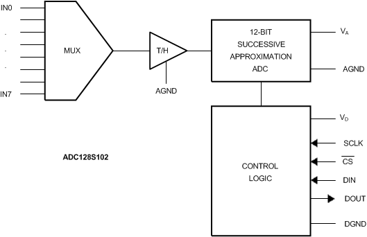
The ADC128S102 device is a low-power, eight-channel CMOS 12-bit analog-to-digital converter specified for conversion throughput rates of 50 kSPS to 1 MSPS. The converter is based on a successive-approximation register architecture with an internal track-and-hold circuit. The device can be configured to accept up to eight input signals at inputs IN0 through IN7.
The output serial data is straight binary and is compatible with several standards, such as SPI, QSPI, MICROWIRE, and many common DSP serial interfaces.
The ADC128S102 may be operated with independent analog and digital supplies. The analog supply (VA) can range from 2.7 V to 5.25 V, and the digital supply (VD) can range from 2.7 V to VA. Normal power consumption using a 3-V or 5-V supply is 2.3 mW and 10.7 mW, respectively. The power-down feature reduces the power consumption to 0.06 µW using a 3-V supply and 0.25 µW using a 5-V supply.
Device Information(1)
- For all available packages, see the orderable addendum at the end of the data sheet.
Block Diagram

4 Revision History
Changes from O Revision (November 2016) to P Revision
- Changed feature link from 5962R07727 to 5962R07227Go
Changes from N Revision (September 2015) to O Revision
- Changed the title of the ADC128S102QML-SP data sheetGo
- Added Radiation Report link to FeaturesGo
- Changed ApplicationsGo
- Changed Device Information table Go
- Added 14-pin CFP package option to the data sheet Go
- Added TYPE column to the Pin Functions table Go
- Added tablenote for digital supply voltage maximums allowed in the Absolute Maximum Ratings tableGo
- Updated maximum tablenote for the digital supply voltage in the Absolute Maximum Ratings tableGo
- Added tablenote for the voltage on any pin to GND maximums allowed in the Absolute Maximum Ratings tableGo
- Added links to the Quality Conformance Inspection table to the Electrical Characteristics tablesGo
- Added MIN and MAX test conditions for the SCLK duty cycle in the Electrical Characteristics: ADC128S102QML-SP Converter tableGo
- Changed ADC128S102 Operational Timing Diagram imageGo
- Changed first sentence and added MIL-STD-883G, Test Method 1019.7 link to the Total Ionizing Dose sectionGo
- Changed total ionizing dose rate from 0.16 to 0.027 rad(Si)/sGo
- Changed Single Event Latch-Up section to Single Event Latch-Up and Functional InterruptGo
- Added sentence to Serial Interface section: Note that CS is asynchronous.Go
- Added Engineering Samples sectionGo
Changes from H Revision (October 2009) to N Revision
- Added Pin Configuration and Functions section, ESD Ratings table, Feature Description section, Device Functional Modes, Application and Implementation section, Power Supply Recommendations section, Layout section, Device and Documentation Support section, and Mechanical, Packaging, and Orderable Information section Go
Changes from G Revision (October 2009) to H Revision
- Added reference to Note 11. Go
- Added Note:11.Go
- Deleted 'TYPICAL' numbers from tDHID, tDS and tDIHGo
- Changed Min limit on tDHID from 11 to 7. Go
Changes from F Revision (June 2009) to G Revision
- Deleted reference to Ta Min and Ta Max under titled sections. Go
Changes from E Revision (April 2009) to F Revision
- Changed AC Electrical Characteristics - SCLK Duty Cycle, typ limits Go
Changes from D Revision (January 2009) to E Revision
- Changed Note 10Go
- Changed spec typo for Clock Frequency rangeGo
- Changed electrical headings from '8 Mhz to 16 Mhz' to '0.8 Mhz and 16 Mhz'.Go
- Reformatted Burn In Delta tableGo
- Added new ENOB vs SCLK Plot Go
Changes from C Revision (November 2008) to D Revision
- Moved Rad information from Key Specifications to FeaturesGo
- Deleted ADC128S102WGMLS referenceGo
- Added Burn In Delta TableGo
Changes from B Revision (August 2008) to C Revision
- Corrected package reference from 16-lead TSSOP to 16-lead Ceramic SOIC, Removed QV NSID reference and Added SMD Number to RQV NSID in Features. Go
Changes from A Revision (August 2008) to B Revision
- Typo, Changed Figure 2, tDIS lower left hand side changed to tDS and tDIH lower left hand side change to tDH in Timing Diagrams. Go