SNOI146C September 2011 – December 2017 ADC141S628-Q1
PRODUCTION DATA.
- 1 Features
- 2 Applications
- 3 Description
- 4 Revision History
- 5 Pin Configuration and Functions
- 6 Specifications
- 7 Detailed Description
- 8 Application and Implementation
- 9 Power Supply Recommendations
- 10Layout
- 11Device and Documentation Support
- 12Mechanical, Packaging, and Orderable Information
1 Features
- Qualified for Automotive Applications
- AEC-Q100 Qualified With the Following Results:
- Device Temperature Grade 2: –40°C to 105°C Ambient Operating Temperature Range
- Device HBM ESD Classification Level H2
- Device CDM ESD Classification Level C6
- 14-Bit Resolution With no Missing Codes
- Specified Performance Up to 200 kSPS
- Pseudo Differential Inputs
- Zero-Power Track Mode
- ±150-mV Swing Around GND on Negative Input
- Separate Digital I/O and Analog Supplies
- Operating Temperature Range of –40°C to +105°C
- SPI™, QSPI™, Microwire, DSP-Compatible Serial Interface
- Conversion Rate: 50 kSPS to 200 kSPS
- INL (–15°C to +65°C): ±0.95 LSB (max)
- DNL: ±0.95 LSB (max)
- Post Calibration TUE (–15°C to +65°C): ±0.5 mV (max)
- SNR: 80 dBc (min)
- THD: –97 dBc (typ)
- ENOB: 13.0 Bits (min)
- Power Consumption:
2 Applications
- Automotive Battery Management
- Automotive Navigation
- Portable Systems
- Medical Instruments
- Instrumentation and Control Systems
- Motor Control
- Direct Sensor Interface
3 Description
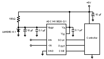
The ADC141S628-Q1 device is a 14-bit, 200-kSPS, pseudo-differential, analog-to-digital converter (ADC) that is AEC-Q100 grade 2 qualified. The converter is based on a successive-approximation register (SAR) architecture and has pseudo-differential analog inputs. The signal path is maintained from the internal sample-and-hold circuits throughout the ADC to provide excellent common-mode noise rejection. The ADC141S628-Q1 features a zero-power track mode where the ADC is consuming the minimum amount of supply current while the internal sampling capacitor tracks the applied analog input voltage.
The serial data output of the ADC141S628-Q1 is straight binary and is compatible with several standards, such as SPI, QSPI, Microwire, and many common DSP serial interfaces. The ADC141S628-Q1 has no latency which means the conversion result is clocked out by the serial clock input and is the result of the conversion currently in progress.
The ADC141S628-Q1 can be operated with independent analog (VA) and digital input/output (VIO) supplies. VA and VIO can range from 4.5 V to 5.5 V and can be set independent of each other. This functionality allows a user to maximize performance and minimize power consumption. Similarly, the ADC141S628-Q1 uses an external reference that can be varied from 1.0 V to VA allowing users to optimize the full dynamic range of the input. The pseudo-differential input, low power consumption, and small size make the ADC141S628-Q1 ideal for remote data acquisition applications.
Operation is specified over the temperature range of –40°C to +105°C and clock rates of 0.36 MHz to 3.6 MHz. The ADC141S628-Q1 is available in a 10-lead package.
Device Information(1)
| PART NUMBER | PACKAGE | BODY SIZE (NOM) |
|---|---|---|
| ADC141S628-Q1 | VSSOP (10) | 3.00 mm × 3.00 mm |
- For all available packages, see the orderable addendum at the end of the data sheet.
4 Revision History
Changes from B Revision (November 2017) to C Revision
- Changed first Features bullet, added AEC-Q100 qualification bullet and sub-bulletsGo
- Changed ADC141S628-Q1 to ADC141S628-Q1 throughout documentGo
- Changed front page figure Go
Changes from A Revision (September 2011) to B Revision
- Added Device Information table, Pin Configuration and Functions section, ESD Ratings table, Thermal Information table, Functional Block Diagram section, Feature Description section, Device Functional Modes section, Application and Implementation section, Power Supply Recommendations section, Layout section, Device and Documentation Support section, and Mechanical, Packaging, and Orderable Information sectionGo
- Changed MSOP to VSSOP throughout document Go
- Changed Pin Out Diagram title from Connection Diagram Go
- Deleted Ordering Information tableGo
- Added I/O column to Pin Functions table Go
- Added maximum specification to Power consumption row of Absolute Maximum Ratings tableGo
- Changed footnote 1 of Absolute Maximum Ratings tableGo
- Changed Operating Ratings table title to Recommended Operating ConditionsGo
- Changed Operating temperature range parameter specifications to min and max specifications from –40 ≤ TA ≤ 105 max specification Go
- Added fSCLK parameter to Recommended Operating Conditions from Operating Conditions section; deleted Operating Conditions sectionGo
- Deleted Package Thermal Resistance table Go
- Added unit to Analog input pin, +IN, Analog input voltage, and Digital input pins voltage range parametersGo
- Deleted footnote 1 from Recommended Operating Conditions table and changed last footnote to include updated link Go
- Changed condition statement of ADC141S628-Q1 Converter Electrical Characteristics table to remove boldface conditionGo
- Changed INL and PCTUE parameter specification test conditions Go
- Added TA = –40°C to +105°C to IDCL parameter test conditions Go
- Changed VA to max specification from typ specification in VREF parameter Go
- Changed fSCLK = 0 to fSCLK = low in IVA (PD), IVIO (PD), and IVREF (PD) parameter test conditionsGo
- Deleted last footnote from ADC141S628-Q1 Converter Electrical Characteristics tableGo
- Changed condition statement of ADC141S628-Q1 Timing Requirements table to remove boldface conditionGo
- Added temperature conditions to certain parameters in the ADC141S628-Q1 Timing Requirements tableGo
- Changed title of Typical Characteristics from Typical Performance Characteristics Go
- Changed Overview title from Functional DescriptionGo
- Deleted last sentence of second paragraph in Reference Input (VREF) sectionGo
- Changed last paragraph of Reference Input (VREF) sectionGo
- Changed Layout Guidelines title from PCB Layout and Circuit ConsiderationsGo
