SBAS531D December 2010 – February 2016 ADS8555
PRODUCTION DATA.
- 1 Features
- 2 Applications
- 3 Description
- 4 Revision History
- 5 Pin Configuration and Functions
-
6 Specifications
- 6.1 Absolute Maximum Ratings
- 6.2 ESD Ratings
- 6.3 Recommended Operating Conditions
- 6.4 Thermal Information
- 6.5 Electrical Characteristics
- 6.6 Serial Interface Timing Requirements
- 6.7 Parallel Interface Timing Requirements (Read Access)
- 6.8 Parallel Interface Timing Requirements (Write Access)
- 6.9 Typical Characteristics
- 7 Detailed Description
- 8 Applications and Implementation
- 9 Power Supply Recommendations
- 10Layout
- 11Device and Documentation Support
- 12Mechanical, Packaging, and Orderable Information
1 Features
- Six SAR ADCs Grouped in Three Pairs
- Maximum Data Rate Per Channel With Internal Clock and Reference:
630 kSPS (Parallel) or 450 kSPS (Serial) - Maximum Data Rate Per Channel With External Clock and Reference:
800 kSPS (Parallel) or 500 kSPS (Serial) - Pin-Selectable or Programmable Input Voltage Ranges: Up to ±12 V
- Excellent AC Performance:
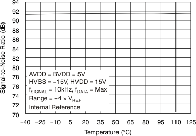
91.5-dB SNR, –94-dB THD - Programmable and Buffered Internal Reference: 0.5 V to 2.5 V and 0.5 V to 3 V
- Comprehensive Power-Down Modes:
- Deep Power Down (Standby Mode)
- Auto-Nap Power Down
- Selectable Parallel or Serial Interface
- Operating Temperature Range: –40°C to 125°C
- LQFP-64 Package
2 Applications
- Power Quality Measurements
- Protection Relays
- Multi-Axis Motor Controls
- Programmable Logic Controllers
- Industrial Data Acquisition
SNR vs Temperature

3 Description
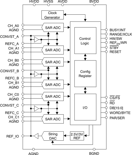
The ADS8555 device contains six low-power, 16-bit, successive approximation register (SAR)-based analog-to-digital converters (ADCs) with true bipolar inputs. Each channel contains a sample-and-hold circuit that allows simultaneous high-speed multi-channel signal acquisition.
The ADS8555 device supports data rates of up to 630 kSPS in parallel interface mode or up to 450 kSPS if the serial interface is used. The bus width of the parallel interface can be set to eight or 16 bits. In serial mode, up to three output channels can be activated.
The ADS8555 device is specified over the extended industrial temperature range of –40°C to 125°C and is available in an LQFP-64 package.
Device Information(1)
| PART NUMBER | PACKAGE | BODY SIZE (NOM) |
|---|---|---|
| ADS8555 | LQFP (64) | 10.00 mm × 10.00 mm |
- For all available packages, see the orderable addendum at the end of the data sheet.
Block Diagram

4 Revision History
Changes from C Revision (October 2015) to D Revision
Changes from B Revision (February 2011) to C Revision
- Added ESD Ratings table, Feature Description section, Device Functional Modes, Application and Implementation section, Power Supply Recommendations section, Layout section, Device and Documentation Support section, and Mechanical, Packaging, and Orderable Information section Go
Changes from A Revision (January 2011) to B Revision
- Changed description of pin 18 in Pin Descriptions tableGo
- Added clarification of INT in BUSY/INT sectionGo
- Updated Table 4Go
- Changed bit C20 in Table 5Go
Changes from * Revision (December 2010) to A Revision