-
CSD16323Q3 N-Channel NexFET™ Power MOSFET
DATA SHEET
CSD16323Q3 N-Channel NexFET™ Power MOSFET
1 Features
- Optimized for 5-V Gate Drive
- Ultra-Low Qg and Qgd
- Low Thermal Resistance
- Avalanche Rated
- Lead-Free Terminal Plating
- RoHS Compliant
- Halogen Free
- SON 3.3-mm × 3.3-mm Plastic Package
2 Applications
- Point-of-Load Synchronous Buck Converter for Applications in Networking, Telecom and Computing Systems
- Optimized for Control or Synchronous FET Applications
3 Description
This 25-V, 3.8-mΩ, 3.3 × 3.3-mm SON NexFET™ power MOSFET has been designed to minimize losses in power conversion and optimized for 5-V gate drive applications.
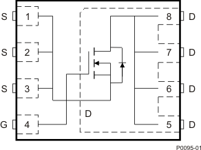
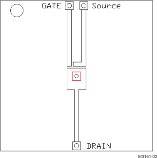
Top View
Product Summary
| TA = 25°C | TYPICAL VALUE | UNIT | ||
|---|---|---|---|---|
| VDS | Drain-to-Source Voltage | 25 | V | |
| Qg | Gate Charge Total (4.5 V) | 6.2 | nC | |
| Qgd | Gate Charge Gate-to-Drain | 1.1 | nC | |
| RDS(on) | Drain-to-Source On Resistance | VGS = 3 V | 5.4 | mΩ |
| VGS = 4.5 V | 4.4 | |||
| VGS = 8 V | 3.8 | |||
| Vth | Threshold Voltage | 1.1 | V | |
Device Information(1)
| DEVICE | MEDIA | QTY | PACKAGE | SHIP |
|---|---|---|---|---|
| CSD16323Q3 | 13-Inch Reel | 2500 | SON 3.30-mm × 3.30-mm Plastic Package |
Tape and Reel |
| CSD16323Q3T | 7-Inch Reel | 250 |
- For all available packages, see the orderable addendum at the end of the data sheet.
Absolute Maximum Ratings
| TA = 25°C (unless otherwise stated) | VALUE | UNIT | |
|---|---|---|---|
| VDS | Drain-to-Source Voltage | 25 | V |
| VGS | Gate-to-Source Voltage | +10 / –8 | V |
| ID | Continuous Drain Current (Package Limit) | 60 | A |
| Continuous Drain Current (Silicon Limited), TC = 25°C | 105 | ||
| Continuous Drain Current(1) | 20 | ||
| IDM | Pulsed Drain Current(2) | 240 | A |
| PD | Power Dissipation(1) | 2.8 | W |
| Power Dissipation, TC = 25°C | 74 | ||
| TJ, Tstg |
Operating Junction, Storage Temperature |
–55 to 150 | °C |
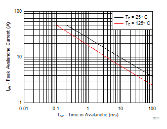
| EAS | Avalanche Energy, Single Pulse ID = 50 A, L = 0.1 mH, RG = 25 Ω |
125 | mJ |
- RθJA = 45°C/W on 1-in2, 2-oz Cu pad on 0.06-in thick FR4 PCB.
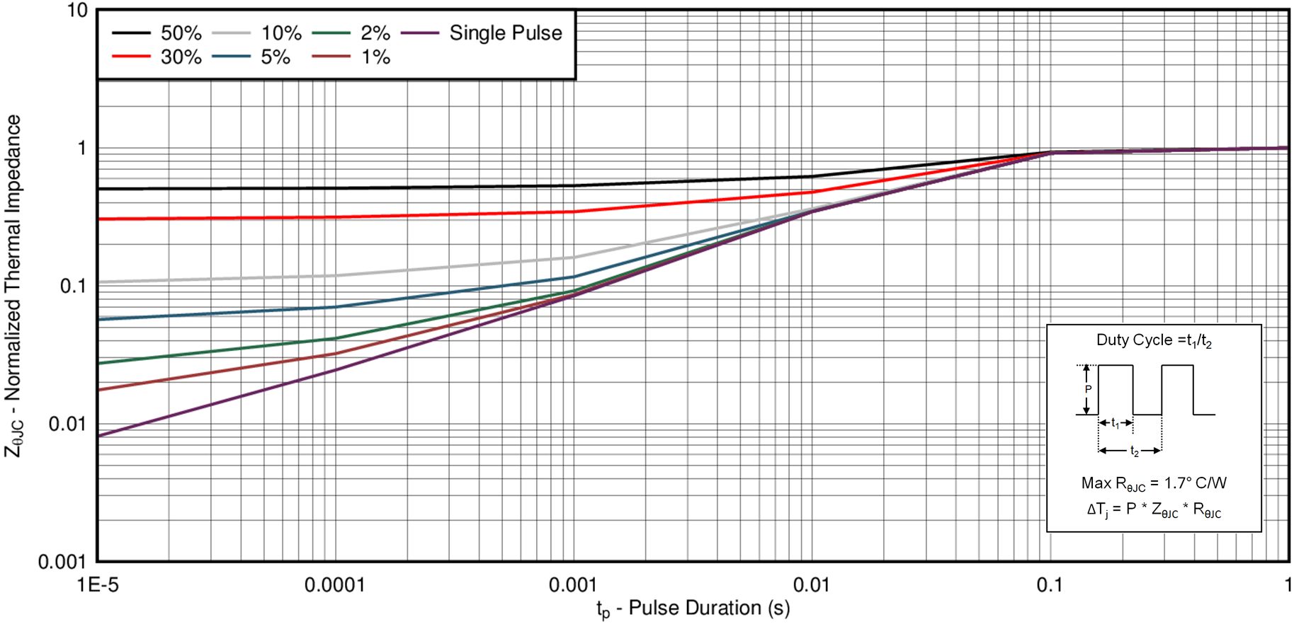
- Max RθJC = 1.7°C/W, pulse duration ≤ 100 μs, duty cycle ≤ 1%.
RDS(on) vs VGS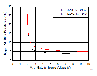 |
Gate Charge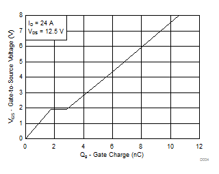 |
4 Revision History
Changes from B Revision (June 2011) to C Revision
- Changed Description textGo
- Added silicon limited continuous drain current to Absolute Maximum Ratings tableGo
- Changed Note 2 in Absolute Maximum Ratings tableGo
- Changed values in the Thermal Information table to align with standardsGo
- Changed Figure 1 to reflect a transient RθJC curveGo
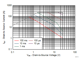
- Changed Figure 10 to reflect measured dataGo
- Added Device and Documentation Support sectionGo
- Changed MECHANICAL DATA section to Mechanical, Packaging, and Orderable Information sectionGo
Changes from A Revision (April 2010) to B Revision
- Replaced the THERMAL CHARACTERISTICS table with the new Thermal Information TableGo
- Replaced Figure 10 - Maximum Safe Operating AreaGo
Changes from * Revision (August 2009) to A Revision
- Changed RDS(on) - VGS = 3 V, ID = 24 A MAX value From: 6.5 To: 7.2Go
5 Specifications
5.1 Electrical Characteristics
TA = 25°C (unless otherwise stated)5.2 Thermal Information
TA = 25°C (unless otherwise stated)| THERMAL METRIC | MIN | TYP | MAX | UNIT | |
|---|---|---|---|---|---|
| RθJC | Junction-to-case thermal resistance(1) | 1.7 | °C/W | ||
| RθJA | Junction-to-ambient thermal resistance(1)(2) | 55 | °C/W | ||
(1) RθJC is determined with the device mounted on a 1-in2 (6.45-cm2), 2-oz (0.071-mm) thick Cu pad on a 1.5-in × 1.5-in (3.81-cm × 3.81-cm), 0.06-in (1.52-mm) thick FR4 PCB. RθJC is specified by design, whereas RθJA is determined by the user’s board design.
(2) Device mounted on FR4 material with 1-in2 (6.45-cm2), 2-oz (0.071-mm) thick Cu.
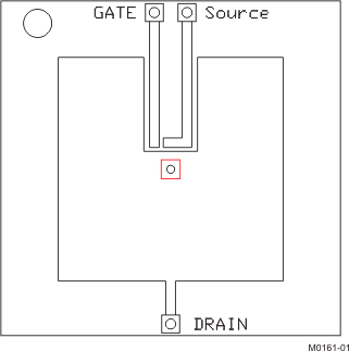 |
Max RθJA = 55°C/W when mounted on 1 in2 of 2-oz Cu. |
 |
Max RθJA = 160°C/W when mounted on minimum pad area of 2-oz Cu. |
5.3 Typical MOSFET Characteristics
TA = 25°C (unless otherwise stated)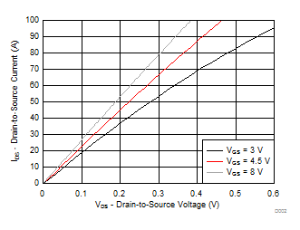
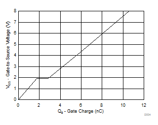
| ID = 24 A | VDS = 12.5 V |
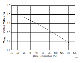
| ID = 250 µA |
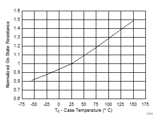
| ID = 24 A | VGS = 4.5 V |
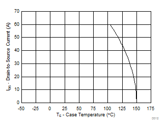
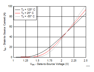
| VDS = 5 V |
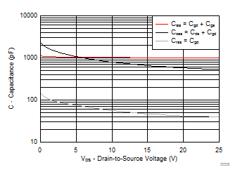
| f = 1 MHz | VGS = 0 V |

| ID = 24 A |
