DATA SHEET
CSD19534Q5A 100V N 通道 NexFET 功率金属氧化物半导体场效应晶体管 (MOSFET)
本资源的原文使用英文撰写。 为方便起见,TI 提供了译文;由于翻译过程中可能使用了自动化工具,TI 不保证译文的准确性。 为确认准确性,请务必访问 ti.com 参考最新的英文版本(控制文档)。
1 特性
- 超低 Qg 和 Qgd
- 低热阻
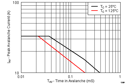
- 雪崩额定值
- 无铅端子镀层
- 符合 RoHS 环保标准
- 无卤素
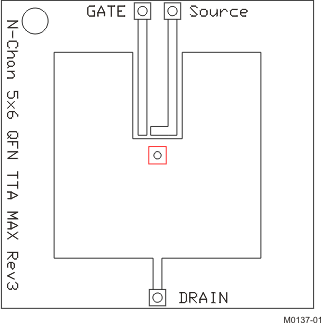
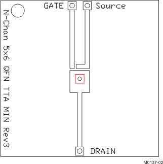
- 小外形尺寸无引线 (SON) 5mm x 6mm 塑料封装
2 应用范围
- 初级侧电信应用
- 电机控制
3 说明
这款 100V,12.6mΩ,SON 5mm x 6mm NexFET™ 功率 MOSFET 被设计成在功率转换应用中最大限度地降低损耗。
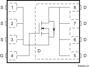
顶视图
米6体育平台手机版_好二三四概要
| TA = 25°C | 典型值 | 单位 | ||
|---|---|---|---|---|
| VDS | 漏源电压 | 100 | V | |
| Qg | 栅极电荷总量 (10V) | 17 | nC | |
| Qgd | 栅漏栅极电荷 | 3.2 | nC | |
| RDS(on) | 漏源导通电阻 | VGS = 6V | 14.1 | mΩ |
| VGS = 10V | 12.6 | mΩ | ||
| VGS(th) | 阀值电压 | 2.8 | V | |
订购信息(1)
| 器件 | 介质 | 数量 | 封装 | 出货 |
|---|---|---|---|---|
| CSD19534Q5A | 13 英寸卷带 | 2500 | SON 5mm x 6mm 塑料封装 |
卷带封装 |
| CSD19534Q5AT | 7 英寸卷带 | 250 |
- 要了解所有可用封装,请见数据表末尾的可订购米6体育平台手机版_好二三四附录。
最大绝对额定值
| TA = 25°C | 值 | 单位 | |
|---|---|---|---|
| VDS | 漏源电压 | 100 | V |
| VGS | 栅源电压 | ±20 | V |
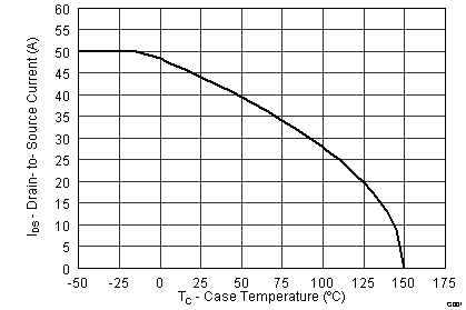
| ID | 持续漏极电流(受封装限制) | 50 | A |
| 持续漏极电流(受芯片限制),TC = 25°C 时测得 | 44 | ||
| 持续漏极电流(1) | 10 | ||
| IDM | 脉冲漏极电流(2) | 137 | A |
| PD | 功率耗散(1) | 3.2 | W |
| 功率耗散,TC = 25°C | 63 | ||
| TJ, Tstg |
运行结温和 储存温度范围 |
-55 至 150 | °C |
| EAS | 雪崩能量,单脉冲 ID = 33A,L = 0.1mH,RG = 25Ω |
55 | mJ |
- RθJA = 40°C/W,这是在一个厚度 0.06 英寸环氧树脂 (FR4) 印刷电路板 (PCB) 上的 1 英寸2,2 盎司 的铜过渡垫片上测得的典型值。
- 最大 RθJC = 2.0°C/W,脉冲持续时间 ≤ 100μs,占空比 ≤ 1%
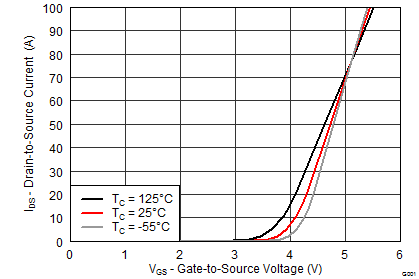
RDS(on) 与 VGS 间的关系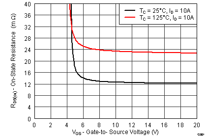 |
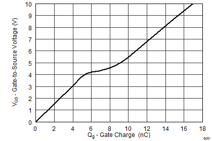
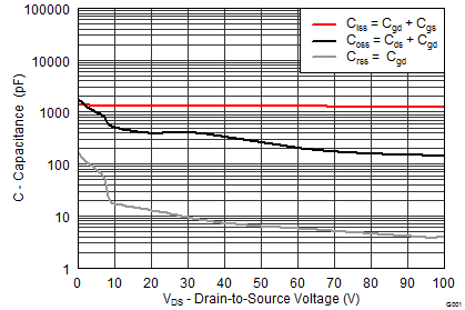
栅极电荷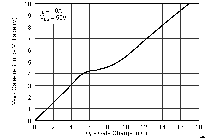 |
4 修订历史记录
| 日期 | 修订版本 | 注释 |
|---|---|---|
| 2014 年 5 月 | * | 最初发布。 |
5 Specifications
5.1 Electrical Characteristics
(TA = 25°C unless otherwise stated)| PARAMETER | TEST CONDITIONS | MIN | TYP | MAX | UNIT | ||
|---|---|---|---|---|---|---|---|
| STATIC CHARACTERISTICS | |||||||
| BVDSS | Drain-to-Source Voltage | VGS = 0 V, ID = 250 μA | 100 | V | |||
| IDSS | Drain-to-Source Leakage Current | VGS = 0 V, VDS = 80 V | 1 | μA | |||
| IGSS | Gate-to-Source Leakage Current | VDS = 0 V, VGS = 20 V | 100 | nA | |||
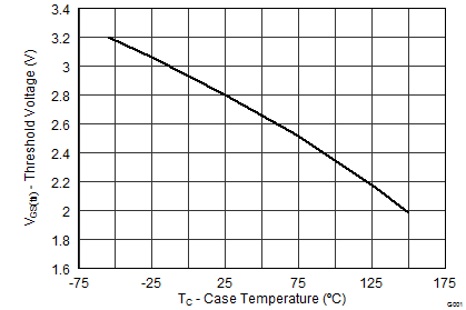
| VGS(th) | Gate-to-Source Threshold Voltage | VDS = VGS, ID = 250 μA | 2.4 | 2.8 | 3.4 | V | |
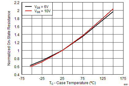
| RDS(on) | Drain-to-Source On Resistance | VGS = 6 V, ID = 10 A | 14.1 | 17.6 | mΩ | ||
| VGS = 10 V, ID = 10 A | 12.6 | 15.1 | mΩ | ||||
| gfs | Transconductance | VDS = 10 V, ID = 10 A | 47 | S | |||
| DYNAMIC CHARACTERISTICS | |||||||
| Ciss | Input Capacitance | VGS = 0 V, VDS = 50 V, f = 1 MHz | 1290 | 1680 | pF | ||
| Coss | Output Capacitance | 257 | 330 | pF | |||
| Crss | Reverse Transfer Capacitance | 5.7 | 7.4 | pF | |||
| RG | Series Gate Resistance | 1.1 | 2.2 | Ω | |||
| Qg | Gate Charge Total (10 V) | VDS = 50 V, ID = 10 A | 17 | 22 | nC | ||
| Qgd | Gate Charge Gate to Drain | 3.2 | nC | ||||
| Qgs | Gate Charge Gate to Source | 5.1 | nC | ||||
| Qg(th) | Gate Charge at Vth | 3.3 | nC | ||||
| Qoss | Output Charge | VDS = 50 V, VGS = 0 V | 44 | nC | |||
| td(on) | Turn On Delay Time | VDS = 50 V, VGS = 10 V, IDS = 10 A, RG = 0 Ω |
9 | ns | |||
| tr | Rise Time | 14 | ns | ||||
| td(off) | Turn Off Delay Time | 20 | ns | ||||
| tf | Fall Time | 6 | ns | ||||
| DIODE CHARACTERISTICS | |||||||
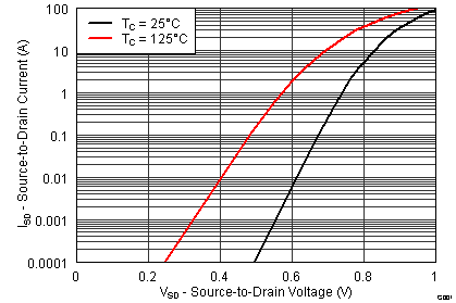
| VSD | Diode Forward Voltage | ISD = 10 A, VGS = 0 V | 0.8 | 1.0 | V | ||
| Qrr | Reverse Recovery Charge | VDS= 50 V, IF = 10 A, di/dt = 300 A/μs |
134 | nC | |||
| trr | Reverse Recovery Time | 53 | ns | ||||
5.2 Thermal Information
(TA = 25°C unless otherwise stated)| PARAMETER | MIN | TYP | MAX | UNIT | |
|---|---|---|---|---|---|
| RθJC | Junction-to-Case Thermal Resistance (1) | 2.0 | °C/W | ||
| RθJA | Junction-to-Ambient Thermal Resistance(1)(2) | 50 | |||
(1) RθJC is determined with the device mounted on a 1-inch2 (6.45-cm2), 2-oz. (0.071-mm thick) Cu pad on a 1.5-inch × 1.5-inch (3.81-cm × 3.81-cm), 0.06-inch (1.52-mm) thick FR4 PCB. RθJC is specified by design, whereas RθJA is determined by the user’s board design.
(2) Device mounted on FR4 material with 1-inch2 (6.45-cm2), 2-oz. (0.071-mm thick) Cu.
 |
Max RθJA = 50°C/W when mounted on 1 inch2 (6.45 cm2) of 2-oz. (0.071-mm thick) Cu. |
 |
Max RθJA = 115°C/W when mounted on a minimum pad area of 2-oz. (0.071-mm thick) Cu. |
5.3 Typical MOSFET Characteristics
(TA = 25°C unless otherwise stated)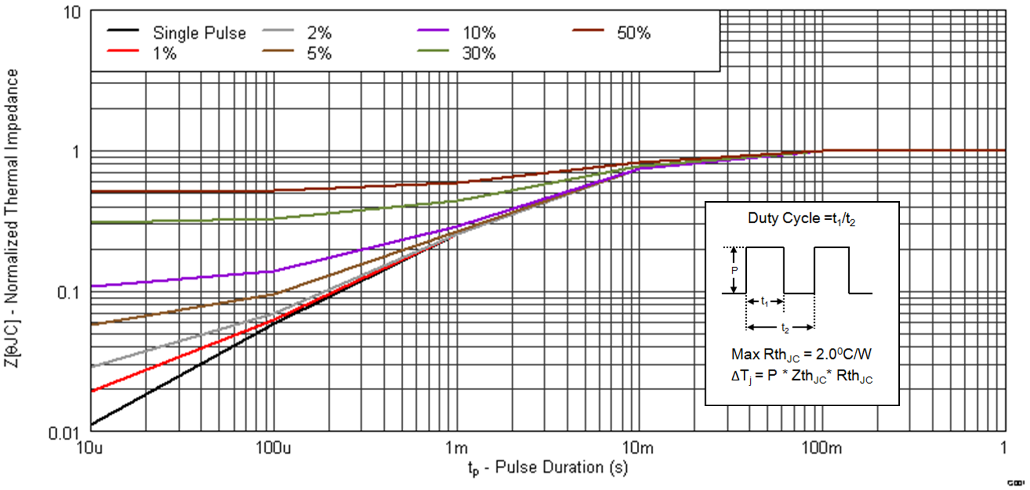
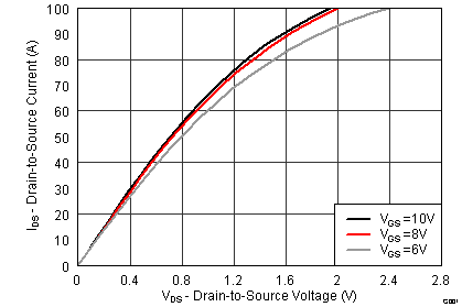
| ID = 10 A | VDS = 50 V | |
| ID = 250 µA | ||
| ID = 10 A | ||
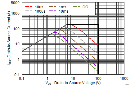
| Single Pulse | Max RθJC = 2.0°C/W | |
| VDS = 5 V | ||
6 器件和文档支持
6.1 Trademarks
NexFET is a trademark of Texas Instruments.
6.2 Electrostatic Discharge Caution

These devices have limited built-in ESD protection. The leads should be shorted together or the device placed in conductive foam during storage or handling to prevent electrostatic damage to the MOS gates.
6.3 Glossary
SLYZ022 — TI Glossary.
This glossary lists and explains terms, acronyms and definitions.