-
LM26LV and LM26LV-Q1 1.6-V, WSON-6 Factory Preset Temperature Switch and Temperature Sensor
- 1 Features
- 2 Applications
- 3 Description
- 4 Revision History
- 5 Pin Configuration and Functions
- 6 Specifications
-
7 Detailed Description
- 7.1 Overview
- 7.2 Functional Block Diagram
- 7.3 Feature Description
- 7.4 Device Functional Modes
- 8 Application and Implementation
- 9 Power Supply Recommendations
- 10Layout
- 11Device and Documentation Support
- 12Mechanical, Packaging, and Orderable Information
- IMPORTANT NOTICE
LM26LV and LM26LV-Q1 1.6-V, WSON-6 Factory Preset Temperature Switch and Temperature Sensor
1 Features
- Low 1.6-V Operation
- Low Quiescent Current
- Latching Function: Device Can Latch the Over Temperature Condition
- Push-Pull and Open-Drain Temperature Switch Outputs
- Wide Trip Point Range of 0°C to 150°C
- Very Linear Analog VTEMP Temperature Sensor Output
- VTEMP Output Short-Circuit Protected
- Accurate Over –50°C to 150°C Temperature Range
- Excellent Power Supply Noise Rejection
- LM26LVQISD-130 and LM26LVQISD-135 are AEC-Q100 Qualified and are Manufactured on an Automotive Grade Flow:
- Device Temperature Grade 0: –40°C to 150°C Ambient Operating Temperature Range
- Device HBM ESD Classification Level 3 A
- Device CDM ESD Classification Level C6
- Device MM ESD Classification Level M3
2 Applications
- Cell Phones and Wireless Transceivers
- Digital Cameras
- Battery Management Systems
- Automotive Applications
- Disk Drives
- Games and Appliances
3 Description
The LM26LV and LM26LV-Q1 are low-voltage, precision, dual-output, low-power temperature switches and temperature sensors. The temperature trip point (TTRIP) can be preset at the factory to any temperature in the range of 0°C to 150°C in 1°C increments. Built-in temperature hysteresis (THYST) keeps the output stable in an environment of temperature instability.
In normal operation the LM26LV or LM26LV-Q1 temperature switch outputs assert when the die temperature exceeds TTRIP. The temperature switch outputs will reset when the temperature falls below a temperature equal to (TTRIP – THYST). The OVERTEMP digital output, is active-high with a push-pull structure, while the OVERTEMP digital output, is active-low with an open-drain structure.
The analog output, VTEMP, delivers an analog output voltage with Negative Temperature Coefficient (NTC).
Driving the TRIP_TEST input high causes the digital outputs to be asserted for in-situ verification and causes the threshold voltage to appear at the VTEMP output pin, which could be used to verify the temperature trip point.
The LM26LV's and LM26LV-Q1's low minimum supply voltage makes them ideal for 1.8-V system designs. The wide operating range, low supply current, and excellent accuracy provide a temperature switch solution for a wide range of commercial and industrial applications.
Device Information(1)
| PART NUMBER | PACKAGE | BODY SIZE (NOM) |
|---|---|---|
| LM26LV, LM26LV-Q1 | WSON (6) | 2.20 mm × 2.50 mm |
- For all available packages, see the orderable addendum at the end of the data sheet.
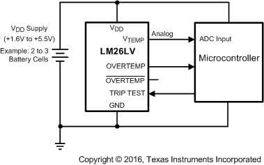
Redundant Protection and Monitoring

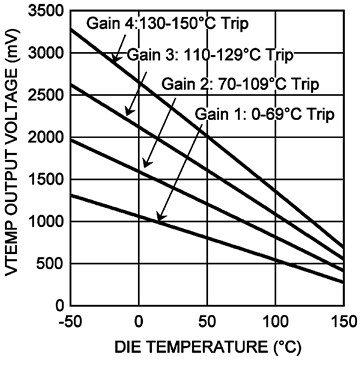
Typical Transfer Characteristic

4 Revision History
Changes from F Revision (February 2013) to G Revision
- Added Device Information table, Pin Configuration and Functions section, Specifications section, ESD Ratings table, Thermal Information table, Switching Characteristics table, Detailed Description section, Application and Implementation section, Power Supply Recommendations section, Layout section, Device and Documentation Support section, and Mechanical, Packaging, and Orderable Information sectionGo
- Updated values in the Thermal Information table to align with JEDEC standardsGo
Changes from E Revision (February 2013) to F Revision
- Changed layout of National Semiconductor Data Sheet to TI formatGo
5 Pin Configuration and Functions
Pin Functions
| PIN | TYPE | DESCRIPTION | EQUIVALENT CIRCUIT | |
|---|---|---|---|---|
| NAME | NO. | |||
| GND | 2 | GND | Power supply ground | — |
| OVERTEMP | 5 | O | Overtemperature switch output. Active high, push-pull. Asserted when the measured temperature exceeds the trip point temperature or if TRIP_TEST = 1. This pin may be left open if not used. |
 |
| OVERTEMP | 3 | O | Overtemperature switch output. Active low, open-drain (See Determining the Pullup Resistor Value). Asserted when the measured temperature exceeds the trip point temperature or if TRIP_TEST = 1. This pin may be left open if not used. |
 |
| TRIP_TEST | 1 | I | TRIP_TEST pin. Active high input. If TRIP_TEST = 0 (Default) then: VTEMP = VTS, temperature sensor output voltage. If TRIP_TEST = 1 then: OVERTEMP and OVERTEMP outputs are asserted and VTEMP = VTRIP, temperature trip voltage. This pin may be left open if not used. |
 |
| VDD | 4 | PWR | Positive supply voltage | — |
| VTEMP | 6 | O | VTEMP analog voltage output. If TRIP_TEST = 0 then: VTEMP = VTS, temperature sensor output voltage. If TRIP_TEST = 1 then: VTEMP = VTRIP, temperature trip voltage. This pin may be left open if not used. |
 |
| Thermal Pad | — | — | The best thermal conductivity between the device and the PCB is achieved by soldering the DAP of the package to the thermal pad on the PCB. The thermal pad can be a floating node. However, for improved noise immunity the thermal pad must be connected to the circuit GND node, preferably directly to pin 2 (GND) of the device. | — |