SNVS316H September 2004 – December 2014 LM2736
PRODUCTION DATA.
- 1 Features
- 2 Applications
- 3 Description
- 4 Revision History
- 5 Pin Configuration and Functions
- 6 Specifications
- 7 Detailed Description
-
8 Application and Implementation
- 8.1 Application Information
- 8.2
Typical Applications
- 8.2.1 LM2736X (1.6 MHz) VBOOST Derived from VIN 5 V to 1.5 V / 750 mA
- 8.2.2 LM2736X (1.6 MHz) VBOOST Derived from VOUT 12 V to 3.3 V / 750 mA
- 8.2.3 LM2736X (1.6 MHz) VBOOST Derived from VSHUNT 18 V to 1.5 V / 750 mA
- 8.2.4 LM2736X (1.6 MHz) VBOOST Derived from Series Zener Diode (VIN) 15 V to 1.5 V / 750 mA
- 8.2.5 LM2736X (1.6 MHz) VBOOST Derived from Series Zener Diode (VOUT) 15 V to 9 V / 750 mA
- 8.2.6 LM2736Y (550 kHz) VBOOST Derived from VIN 5 V to 1.5 V / 750 mA
- 8.2.7 LM2736Y (550 kHz) VBOOST Derived from VOUT 12 V to 3.3 V / 750 mA
- 8.2.8 LM2736Y (550 kHz) VBOOST Derived from VSHUNT 18 V to 1.5 V / 750 mA
- 8.2.9 LM2736Y (550 kHz) VBOOST Derived from Series Zener Diode (VIN) 15 V to 1.5 V / 750 mA
- 8.2.10 LM2736Y (550 kHz) VBOOST Derived from Series Zener Diode (VOUT) 15 V to 9 V / 750 mA
- 9 Power Supply Recommendations
- 10Layout
- 11Device and Documentation Support
- 12Mechanical, Packaging, and Orderable Information
1 Features
- Thin SOT-6 Package
- 3.0 V to 18 V Input Voltage Range
- 1.25 V to 16 V Output Voltage Range
- 750 mA Output Current
- 550 kHz (LM2736Y) and 1.6 MHz (LM2736X) Switching Frequencies
- 350 mΩ NMOS Switch
- 30 nA Shutdown Current
- 1.25 V, 2% Internal Voltage Reference
- Internal Soft-Start
- Current-Mode, PWM Operation
- WEBENCH® Online Design Tool
- Thermal Shutdown
2 Applications
- Local Point of Load Regulation
- Core Power in HDDs
- Set-Top Boxes
- Battery Powered Devices
- USB Powered Devices
- DSL Modems
- Notebook Computers
3 Description
The LM2736 regulator is a monolithic, high frequency, PWM step-down DC/DC converter in a 6-pin Thin SOT package. It provides all the active functions to provide local DC/DC conversion with fast transient response and accurate regulation in the smallest possible PCB area.
With a minimum of external components and online design support through WEBENCH®, the LM2736 is easy to use. The ability to drive 750 mA loads with an internal 350 mΩ NMOS switch using state-of-the-art 0.5 µm BiCMOS technology results in the best power density available. The world class control circuitry allows for on-times as low as 13 ns, thus supporting exceptionally high frequency conversion over the entire 3 V to 18 V input operating range down to the minimum output voltage of 1.25 V. Switching frequency is internally set to 550 kHz (LM2736Y) or 1.6 MHz (LM2736X), allowing the use of extremely small surface mount inductors and chip capacitors. Even though the operating frequencies are very high, efficiencies up to 90% are easy to achieve. External shutdown is included, featuring an ultra-low stand-by current of 30 nA. The LM2736 utilizes current-mode control and internal compensation to provide high-performance regulation over a wide range of operating conditions. Additional features include internal soft-start circuitry to reduce inrush current, pulse-by-pulse current limit, thermal shutdown, and output over-voltage protection.
Device Information(1)
| PART NUMBER | PACKAGE | BODY SIZE (NOM) |
|---|---|---|
| LM2736 | SOT (6) | 2.90 mm x 1.60 mm |
- For all available packages, see the orderable addendum at the end of the datasheet.
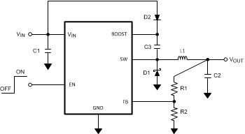
Typical Application Circuit

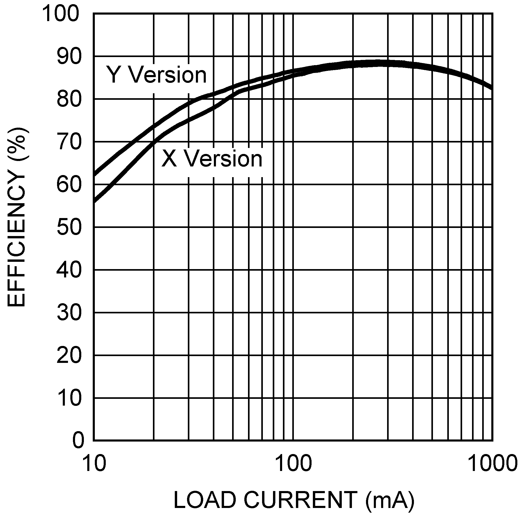
Efficiency vs. Load Current "X"
VIN = 5 V, VOUT = 3.3 V
