-
LM3409, -Q1, LM3409HV, -Q1 P-FET Buck Controller for High-Power LED Drivers
- 1 Features
- 2 Applications
- 3 Description
- 4 Revision History
- 5 Device Comparison Table
- 6 Pin Configuration and Functions
- 7 Specifications
-
8 Detailed Description
- 8.1 Overview
- 8.2 Functional Block Diagram
- 8.3 Feature Description
- 8.4 Device Functional Modes
-
9 Application and Implementation
- 9.1
Application Information
- 9.1.1 Input Undervoltage Lockout (UVLO)
- 9.1.2 Operation Near Dropout
- 9.1.3 LED Ripple Current
- 9.1.4 Buck Converters without Output Capacitors
- 9.1.5 Buck Converters With Output Capacitors
- 9.1.6 Output Overvoltage Protection
- 9.1.7 Input Capacitors
- 9.1.8 P-Channel MOSFET (PFET)
- 9.1.9 Re-Circulating Diode
- 9.2
Typical Applications
- 9.2.1 EN PIN PWM Dimming Application for 10 LEDs
- 9.2.2 Analog Dimming Application for 4 LEDs
- 9.2.3 LM3409 Buck Converter Application
- 9.1
Application Information
- 10Power Supply Recommendations
- 11Layout
- 12Device and Documentation Support
- 13Mechanical, Packaging, and Orderable Information
- IMPORTANT NOTICE
封装选项
机械数据 (封装 | 引脚)
散热焊盘机械数据 (封装 | 引脚)
- DGQ|10
订购信息
LM3409, -Q1, LM3409HV, -Q1 P-FET Buck Controller for High-Power LED Drivers
1 Features
- LM3409-Q1 and LM3409HV-Q1 are Automotive Grade Products: AEC-Q100 Grade 1 Qualified
- 2-Ω, 1-A Peak MOSFET Gate Drive
- VIN Range: 6 V to 42 V (LM3409, LM3409-Q1)
- VIN Range: 6 V to 75 V (LM3409HV, LM3409HV-Q1)
- Differential, High-Side Current Sense
- Cycle-by-Cycle Current Limit
- No Control Loop Compensation Required
- 10,000:1 PWM Dimming Range
- 250:1 Analog Dimming Range
- Supports All-Ceramic Output Capacitors and Capacitor-less Outputs
- Low-Power Shutdown and Thermal Shutdown
- Thermally Enhanced 10-Pin, HVSSOP Package
2 Applications
- LED Driver
- Constant Current Source
- Automotive Lighting
- General Illumination
3 Description
The LM3409, LM3409-Q1, LM3409HV, and LM3409HV-Q1 are P-channel MOSFET (PFET) controllers for step-down (buck) current regulators. They offer wide input voltage range, high-side differential current sense with low adjustable threshold voltage and fast output enable/disable function and a thermally enhanced 10-pin, HVSSOP package. These features combine to make the LM3409 family of devices ideal for use as constant current sources for driving LEDs where forward currents up to 5 A are easily achievable.
The LM3409 devices use constant off-time (COFT) control to regulate an accurate constant current without the need for external control loop compensation. Analog and PWM dimming are easy to implement and result in a highly linear dimming range with excellent achievable contrast ratios. Programmable UVLO, low-power shutdown, and thermal shutdown complete the feature set.
Device Information(1)
| PART NUMBER | PACKAGE | BODY SIZE (NOM) |
|---|---|---|
| LM3409 | HVSSOP (10) | 3.00 mm × 3.00 mm |
| PDIP (14) | 19.177 mm × 6.35 mm | |
| LM3409-Q1 | HVSSOP (10) | 3.00 mm × 3.00 mm |
| LM3409HV | ||
| LM3409HV-Q1 |
- For all available packages, see the orderable addendum at the end of the data sheet.
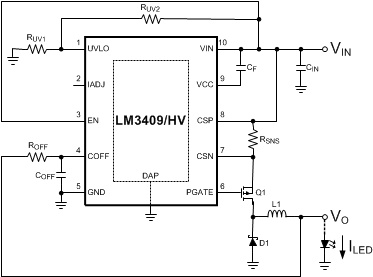
Typical Application Schematic

4 Revision History
Changes from K Revision (July 2014) to L Revision
- Corrected package family reference in Features sectionGo
- Corrected package family reference in Device Information tableGo
- Added Device Comparison tableGo
- Corrected typographical error in package name reference in Pin Configuration and Functions sectionGo
- Corrected typographical error in Absolute Maximum Ratings tableGo
- Corrected typographical error in package name reference in ESD Ratings tableGo
- Corrected package family reference in Thermal Information tableGo
Changes from J Revision (May 2013) to K Revision
- Added ESD Ratings table, Feature Description section, Device Functional Modes, Application and Implementation section, Power Supply Recommendations section, Layout section, Device and Documentation Support section, and Mechanical, Packaging, and Orderable Information sectionGo
Changes from I Revision (May 2013) to J Revision
- Changed layout of National Data Sheet to TI format Go