SNVS616H April 2009 – July 2015 LM3429 , LM3429-Q1
PRODUCTION DATA.
- 1 Features
- 2 Applications
- 3 Description
- 4 Revision History
- 5 Pin Configuration and Functions
- 6 Specifications
-
7 Detailed Description
- 7.1 Overview
- 7.2 Functional Block Diagram
- 7.3
Feature Description
- 7.3.1 Current Regulators
- 7.3.2 Predictive Off-Time (PRO) Control
- 7.3.3 Switching Frequency
- 7.3.4 Average LED Current
- 7.3.5 Analog Dimming
- 7.3.6 Current Sense and Current Limit
- 7.3.7 Control Loop Compensation
- 7.3.8 Output Overvoltage Lockout (OVLO)
- 7.3.9 Input Undervoltage Lockout (UVLO)
- 7.3.10 PWM Dimming
- 7.3.11 Startup Regulator (VCC LDO)
- 7.3.12 Thermal Shutdown
- 7.4 Device Functional Modes
-
8 Application and Implementation
- 8.1 Application Information
- 8.2
Typical Applications
- 8.2.1
Basic Topology Schematics
- 8.2.1.1 Design Requirements
- 8.2.1.2
Detailed Design Procedure
- 8.2.1.2.1 Operating Point
- 8.2.1.2.2 Switching Frequency
- 8.2.1.2.3 Average LED Current
- 8.2.1.2.4 Inductor Ripple Current
- 8.2.1.2.5 LED Ripple Current
- 8.2.1.2.6 Peak Current Limit
- 8.2.1.2.7 Loop Compensation
- 8.2.1.2.8 Input Capacitance
- 8.2.1.2.9 NFET
- 8.2.1.2.10 Diode
- 8.2.1.2.11 Output OVLO
- 8.2.1.2.12 Input UVLO
- 8.2.1.2.13 PWM Dimming Method
- 8.2.1.2.14 Analog Dimming Method
- 8.2.2
Buck-Boost Application - 6 LEDs at 1 A
- 8.2.2.1 Design Requirements
- 8.2.2.2
Detailed Design Procedure
- 8.2.2.2.1 Operating Point
- 8.2.2.2.2 Switching Frequency
- 8.2.2.2.3 Average LED Current
- 8.2.2.2.4 Inductor Ripple Current
- 8.2.2.2.5 Output Capacitance
- 8.2.2.2.6 Peak Current Limit
- 8.2.2.2.7 Loop Compensation
- 8.2.2.2.8 Input Capacitance
- 8.2.2.2.9 NFET
- 8.2.2.2.10 Diode
- 8.2.2.2.11 Input UVLO
- 8.2.2.2.12 Output OVLO
- 8.2.2.3 Application Curve
- 8.2.3 Boost PWM Dimming Application - 9 LEDs at 1 A
- 8.2.4 Buck-Boost Analog Dimming Application - 4 LEDs at 2A
- 8.2.5 Boost Analog Dimming Application - 12 LEDs at 700 mA
- 8.2.6 Buck-Boost PWM Dimming Application - 6 LEDs at 500 mA
- 8.2.7 Buck Application - 3 LEDS at 1.25 A
- 8.2.8 Buck-Boost Thermal Foldback Application - 8 LEDs at 2.5 A
- 8.2.9 SEPIC Application - 5 LEDs at 750 mA
- 8.2.1
Basic Topology Schematics
- 9 Power Supply Recommendations
- 10Layout
- 11Device and Documentation Support
- 12Mechanical, Packaging, and Orderable Information
1 Features
- LM3429-Q1 is AEC-Q100 Grade 1 Qualified for Automotive Applications
- VIN Range From 4.5 V to 75 V
- Adjustable Current Sense Voltage
- High-Side Current Sensing
- 2-Ω, 1-A Peak MosFET Gate Driver
- Input Undervoltage Protection
- Overvoltage Protection
- PWM Dimming
- Analog Dimming
- Cycle-by-Cycle Current Limit
- Programmable Switching Frequency
- Low Profile 14-lead HTSSOP Package
- Thermal Shutdown
2 Applications
- LED Drivers - Buck, Boost, Buck-Boost, SEPIC
- Indoor and Outdoor SSL
- Automotive
- General Illumination
- Constant-Current Regulators
3 Description
The LM3429 is a versatile high voltage N-channel MosFET controller for LED drivers. It can be easily configured in buck, boost, buck-boost and SEPIC topologies. This flexibility, along with an input voltage rating of 75V, makes the LM3429 ideal for illuminating LEDs in a very diverse, large family of applications.
Adjustable high-side current sense voltage allows for tight regulation of the LED current with the highest efficiency possible. The LM3429 uses Predictive Off-time (PRO) control, which is a combination of peak current-mode control and a predictive off-timer. This method of control eases the design of loop compensation while providing inherent input voltage feed-forward compensation.
The LM3429 includes a high-voltage startup regulator that operates over a wide input range of 4.5 V to 75 V. The internal PWM controller is designed for adjustable switching frequencies of up to 2 MHz, thus enabling compact solutions. Additional features include analog dimming, PWM dimming, overvoltage protection, undervoltage lock-out, cycle-by-cycle current limit, and thermal shutdown.
Device Information(1)
| PART NUMBER | PACKAGE | BODY SIZE (NOM) |
|---|---|---|
| LM3429 | HTSSOP (14) | 5.00 mm × 4.40 mm |
| LM3429-Q1 |
- For all available packages, see the orderable addendum at the end of the data sheet.
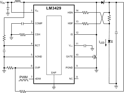
Typical Boost Application Circuit
