-
LM5030 100-V Push-Pull Current Mode PWM Controller
- 1 Features
- 2 Applications
- 3 Description
- 4 Revision History
- 5 Pin Configuration and Functions
- 6 Specifications
- 7 Detailed Description
- 8 Application and Implementation
- 9 Power Supply Recommendations
- 10Layout
- 11Device and Documentation Support
- 12Mechanical, Packaging, and Orderable Information
- IMPORTANT NOTICE
DATA SHEET
LM5030 100-V Push-Pull Current Mode PWM Controller
1 Features
- Internal High-Voltage Start-Up Regulator
- Single Resistor Oscillator Setting
- Synchronizable
- Error Amplifier
- Precision Reference
- Adjustable Softstart
- Dual Mode Overcurrent Protection
- Slope Compensation
- Direct Optocoupler Interface
- 1.5-A Peak Gate Drivers
- Thermal Shutdown
2 Applications
- Telecommunication Power Converters
- Industrial Power Converters
- +42-V Automotive Systems
3 Description
The LM5030 high-voltage PWM controller contains all of the features needed to implement push-pull and bridge topologies, using current-mode control in a small 10-pin package. This device provides two alternating gate driver outputs. The LM5030 includes a high-voltage start-up regulator that operates over a wide input range of 14 V to 100 V. Additional features include: error amplifier, precision reference, dual mode current limit, slope compensation, softstart, sync capability, and thermal shutdown. This high speed IC has total propagation delays less than
100 ns and a 1-MHz capable single-resistor adjustable oscillator.
Device Information(1)
| PART NUMBER | PACKAGE | BODY SIZE (NOM) |
|---|---|---|
| LM5030 | VSSOP (10) | 3.00 mm × 3.00 mm |
| WSON (10) | 4.00 mm × 4.00 mm |
- For all available packages, see the orderable addendum at the end of the data sheet.
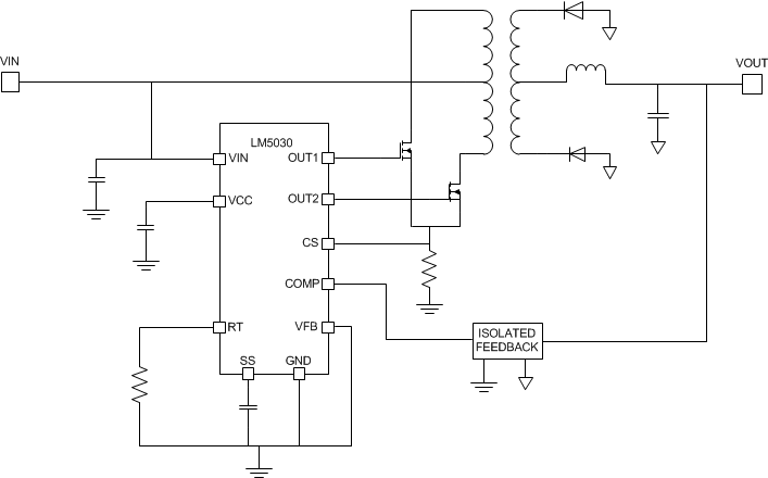
Typical Application Diagram

4 Revision History
Changes from C Revision (March 2013) to D Revision
- Added ESD Ratings table, Thermal Information table, Feature Description section, Device Functional Modes, Application and Implementation section, Power Supply Recommendations section, Layout section, Device and Documentation Support section, and Mechanical, Packaging, and Orderable Information sectionGo
Changes from B Revision (March 2013) to C Revision
- Changed layout of National Data Sheet to TI formatGo
5 Pin Configuration and Functions
DGS, DPR Package
10-Pin VSSOP, WSON
Top View

Pin Functions
| PIN | I/O | DESCRIPTION | APPLICATION INFORMATION | |
|---|---|---|---|---|
| NAME | NO. | |||
| COMP | 3 | O | Output to the error amplifier | There is an internal 5-kΩ pullup resistor on this pin. The error amplifier provides an active sink. |
| CS | 8 | I | Current sense input | Current sense input for current mode control and current limit sensing. Using separate dedicated comparators, if CS exceeds 0.5 V, the outputs will go into cycle-by-cycle current limit. If CS exceeds 0.625 V the outputs will be disabled and a softstart commenced. |
| GND | 7 | — | Return | Ground |
| OUT1 | 5 | O | Output of the PWM controller | Alternating PWM output gate driver |
| OUT2 | 6 | O | Output of the PWM controller | Alternating PWM output gate driver |
| RT | 9 | I | Oscillator timing resistor pin and synchronization input | An external resistor sets the oscillator frequency. This pin will also accept synchronization pulses from an external oscillator. |
| SS | 10 | I | Dual purpose soft start and shutdown pin | A 10-µA current source and an external capacitor set the softstart timing length. The controller will enter a low power state if the SS pin is pulled below the typical shutdown threshold of 0.45 V. |
| VIN | 1 | I | Source input voltage | Input to start-up regulator. Input range 14 to 100 V. |
| VFB | 2 | I | Inverting input to the error amplifier | The non-inverting input is internally connected to a 1.25-V reference. |
| VCC | 4 | I/O | Output from the internal high-voltage series pass regulator. The regulation setpoint is 7.7 V. |
If an auxiliary winding raises the voltage on this pin above the regulation setpoint, the internal series pass regulator will shutdown, reducing the IC power dissipation. |
| WSON DAP |
SUB | — | Die substrate | The exposed die attach pad on the WSON package should be connected to a PCB thermal pad at ground potential. For additional information on using TI's No Pull Back WSON package, refer to WSON Application Note AN-1187 (SNOA401). |