SNOSD65 June 2017 LMH6644-MIL
PRODUCTION DATA.
- 1 Features
- 2 Applications
- 3 Description
- 4 Revision History
- 5 Description (continued)
- 6 Pin Configuration and Functions
- 7 Specifications
- 8 Detailed Description
- 9 Application and Implementation
- 10Power Supply Recommendations
- 11Layout
- 12Device and Documentation Support
- 13Mechanical, Packaging, and Orderable Information
1 Features
- –3 dB BW (AV = +1) 130 MHz
- Supply Voltage Range 2.7 V to 12.8 V
- Slew Rate, (AV = –1) 130 V/µs(1)
- Supply Current (no load) 2.7 mA/amp
- Output Short Circuit Current +115 mA to 145 mA
- Linear Output Current ±75 mA
- Input Common Mode Voltage 0.5 V Beyond V–, 1 V from V+
- Output Voltage Swing 40 mV from Rails
- Input Voltage Noise (100 kHz) 17 nV/√Hz
- Input Current Noise (100 kHz) 0.9 pA/√Hz
- THD (5 MHz, RL = 2 kΩ, VO = 2 VPP, AV = +2) –62 dBc
- Settling Time 68 ns
- Fully Characterized for 3 V, 5 V, and ±5 V
- Overdrive Recovery 100 ns
- Output Short Circuit Protected(2)
- No Output Phase Reversal with CMVR Exceeded
(VS = ±5 V, TA = 25°C, RL = 2 kΩ, AV = +1. Typical Values Unless Specified).
2 Applications
- Active Filters
- CD/DVD ROM
- ADC Buffer Amp
- Portable Video
- Current Sense Buffer
3 Description
The LMH6644-MIL true single supply voltage feedback amplifier offers high speed (130 MHz), low distortion (–62 dBc), and exceptionally high-output current (approximately 75 mA) at low cost and with reduced power consumption when compared against existing devices with similar performance.
Input common mode voltage range extends to 0.5 V below V– and 1 V from V+. Output voltage range extends to within 40 mV of either supply rail, allowing wide dynamic range especially desirable in low-voltage applications. The output stage is capable of approximately 75 mA in order to drive heavy loads. Fast output slew rate (130 V/µs) ensures large peak-to-peak output swings can be maintained even at higher speeds, resulting in exceptional full power bandwidth of 40 MHz with a 3-V supply. These characteristics, along with low cost, are ideal features for a multitude of industrial and commercial applications.
Device Information(1)
| PART NUMBER | PACKAGE | BODY SIZE (NOM) |
|---|---|---|
| LMH6644-MIL | SOIC (14) | 8.64 mm × 3.91 mm |
| TSSOP (14) | 5.00 mm × 4.40 mm |
- For all available packages, see the orderable addendum at the end of the datasheet.
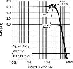
Closed Loop Gain vs Frequency
for Various Supplies

4 Revision History
| DATE | REVISION | NOTES |
|---|---|---|
| June 2017 | * | Initial release. |