SNVS137I March 1999 – September 2015 LP2986
PRODUCTION DATA.
- 1 Features
- 2 Applications
- 3 Description
- 4 Revision History
- 5 Pin Configuration and Function
- 6 Specifications
- 7 Detailed Description
- 8 Application and Implementation
- 9 Power Supply Recommendations
- 10Layout
- 11Device and Documentation Support
- 12Mechanical, Packaging, and Orderable Information
封装选项
机械数据 (封装 | 引脚)
散热焊盘机械数据 (封装 | 引脚)
订购信息
1 Features
- Wide Supply Voltage Range (16 V Maximum)
- Ultra-Low-Dropout Voltage
- 0.5% Output Voltage Accuracy (A Grade)
- Ensured 200-mA Output Current
- < 1-μA Quiescent Current when Shutdown
- Low GROUND Pin Current at All Loads
- High Peak Current Capability (400 mA Typical)
- Overtemperature/Overcurrent Protection
- −40°C to +125°C Junction Temperature Range
2 Applications
- Cellular Phones
- Palmtop/Laptop Computers
- Camcorders, Personal Stereos, Cameras
3 Description
The LP2986 is a 200-mA high-precision LDO regulator with a wide input voltage supply. The device has two output voltage modes: a fixed-precision output mode and an adjustable output voltage via an external resistive divider.
Using an optimized Vertically Integrated PNP (VIP) process, the LP2986 delivers superior performance:
- Dropout Voltage: Typically 180 mV at 200-mA load, and 1 mV at 1-mA load.
- GROUND Pin Current: Typically 1 mA at 200-mA load, and 200 μA at 10-mA load.
- Sleep Mode: The LP2986 draws less than 1 μA quiescent current when SHUTDOWN pin is pulled low.
- ERROR Flag: The built-in ERROR flag goes low when the output drops approximately 5% below nominal.
- Precision Output: The standard product versions available can be pin-strapped (using the internal resistive divider) to provide output voltages of 5 V, 3.3 V, or 3 V with ensured accuracy of 0.5% (A grade) and 1% (standard grade) at room temperature.
Device Information(1)
| PART NUMBER | PACKAGE | BODY SIZE (NOM) |
|---|---|---|
| LP2986 | SOIC (8) | 4.90 mm × 3.91 mm |
| VSSOP (8) | 3.00 mm × 3.00 mm | |
| WSON (8) | 4.00 mm × 4.00 mm |
- For all available packages, see the orderable addendum at the end of the data sheet.
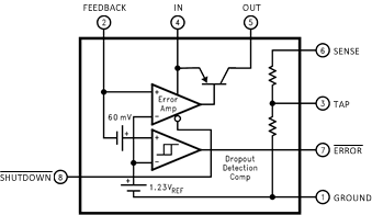
Simplified Schematic
