SLLS632C December 2005 – February 2015 SN65HVD1050
PRODUCTION DATA.
- 1 Features
- 2 Applications
- 3 Description
- 4 Revision History
- 5 Description (Continued)
- 6 Pin Configuration and Functions
-
7 Specifications
- 7.1 Absolute Maximum Ratings
- 7.2 ESD Ratings
- 7.3 Recommended Operating Conditions
- 7.4 Thermal Information
- 7.5 Driver Electrical Characteristics
- 7.6 Receiver Electrical Characteristics
- 7.7 Device Switching Characteristics
- 7.8 Driver Switching Characteristics
- 7.9 Receiver Switching Characteristics
- 7.10 Supply Current
- 7.11 S-Pin Characteristics
- 7.12 VREF-Pin Characteristics
- 7.13 Typical Characteristics
- 8 Parameter Measurement Information
- 9 Detailed Description
- 10Application and Implementation
- 11Power Supply Recommendations
- 12Layout
- 13Device and Documentation Support
- 14Mechanical, Packaging, and Orderable Information
1 Features
- Improved Replacement for the TJA1050
- High Electromagnetic Immunity (EMI)
- Very Low Electromagnetic Emissions (EME)
- Meets or Exceeds the Requirements of
ISO 11898-2 - CAN Bus-Fault Protection of –27 V to 40 V
- Dominant Time-Out Function
- Power-Up and Power-Down Glitch-Free CAN Bus Inputs and Outputs
- High Input Impedance With Low VCC
- Monotonic Outputs During Power Cycling
2 Applications
- Industrial Automation
- DeviceNet™ Data Buses (Vendor ID #806)
- SAE J2284 High-Speed CAN Bus for Automotive Applications
- SAE J1939 Standard Data Bus Interface
- ISO 11783 Standard Data Bus Interface
- NMEA 2000 Standard Data Bus Interface
3 Description
The SN65HVD1050 meets or exceeds the specifications of the ISO 11898 standard for use in applications employing a Controller Area Network (CAN).
As a CAN transceiver, this device provides differential transmit capability to the bus and differential receive capability to a CAN controller at signaling rates up to 1 megabit per second (Mbps)
The SN65HVD1050 is designed for operation in especially harsh environments. As a result, the device features cross-wire, overvoltage and loss of ground protection from –27 V to 40 V, overtemperature shutdown, a –12-V to 12-V common-mode range, and will withstand voltage transients from –200 V to 200 V according to ISO 7637.
Device Information(1)
| PART NUMBER | PACKAGE | BODY SIZE (NOM) |
|---|---|---|
| SN65HVD1050 | SOIC (8) | 4.90 mm × 3.91 mm |
- For all available packages, see the orderable addendum at the end of the data sheet.
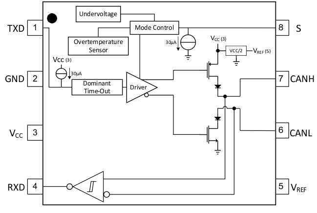
Functional Block Diagram
