SCDS019M May 1995 – December 2015 SN74CBT3251
PRODUCTION DATA.
- 1 Features
- 2 Applications
- 3 Description
- 4 Revision History
- 5 Pin Configuration and Functions
- 6 Specifications
- 7 Parameter Measurement Information
- 8 Detailed Description
- 9 Application and Implementation
- 10Power Supply Recommendations
- 11Layout
- 12Device and Documentation Support
- 13Mechanical, Packaging, and Orderable Information
封装选项
请参考 PDF 数据表获取器件具体的封装图。
机械数据 (封装 | 引脚)
- PW|16
- DB|16
- DBQ|16
- RGY|16
- D|16
散热焊盘机械数据 (封装 | 引脚)
- RGY|16
订购信息
1 Features
2 Applications
- Digital Radio
- Signal Gating
- Factory Automation
- Televisions
- Appliances
- Programmable Logic Circuits
- Sensors
3 Description
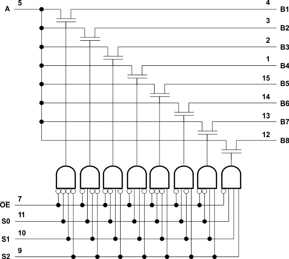
The SN74CBT3251 is a 1-of-8 high-speed TTL-compatible FET multiplexer and demultiplexer. The low ON-state resistance of the switch allows connections to be made with minimal propagation delay.
When output enable (OE) is low, the SN74CBT3251 is enabled, and S0, S1, and S2 select one of the B outputs for the A-input data.
Device Information(1)
| PART NUMBER | PACKAGE | BODY SIZE (NOM) |
|---|---|---|
| SN74CBT3251RGY | VQFN (16) | 3.50 mm × 4.00 mm |
| SN74CBT3251DBQ | SSOP (16) | 3.90 mm × 4.90 mm |
| SN74CBT3251PW | TSSOP (16) | 4.40 mm × 5.00 mm |
| SN74CBT3251DB | SSOP (16) | 5.30 mm × 6.20 mm |
| SN74CBT3251D | SOIC (16) | 3.91 mm × 9.90 mm |
- For all available packages, see the orderable addendum at the end of the data sheet.
Functional Diagram of the SN74CBT3251
