-
SN74LVC1G32 Single 2-Input Positive-OR Gate
- 1 Features
- 2 Applications
- 3 Description
- 4 Revision History
- 5 Pin Configuration and Functions
-
6 Specifications
- 6.1 Absolute Maximum Ratings
- 6.2 ESD Ratings
- 6.3 Recommended Operating Conditions
- 6.4 Thermal Information
- 6.5 Electrical Characteristics
- 6.6 Switching Characteristics, CL = 15 pF
- 6.7 Switching Characteristics, 1.8 V and 2.5V
- 6.8 Switching Characteristics, 3.3 V and 5 V
- 6.9 Operating Characteristics
- 6.10 Typical Characteristics
- 7 Parameter Measurement Information
- 8 Detailed Description
- 9 Application and Implementation
- 10Power Supply Recommendations
- 11Layout
- 12Device and Documentation Support
- 13Mechanical, Packaging, and Orderable Information
- 14Package Option Addendum
- IMPORTANT NOTICE
封装选项
请参考 PDF 数据表获取器件具体的封装图。
机械数据 (封装 | 引脚)
- DPW|5
- DBV|5
- DSF|6
- DCK|5
- DRL|5
- YZP|5
- DRY|6
散热焊盘机械数据 (封装 | 引脚)
订购信息
SN74LVC1G32 Single 2-Input Positive-OR Gate
1 Features
- Available in the Ultra-Small 0.64 mm2
Package (DPW) with 0.5-mm Pitch - Supports 5-V VCC Operation
- Inputs Accept Voltages to 5.5-V
- Supports Down Translation to VCC
- Max tpd of 3.6 ns at 3.3-V
- Low Power Consumption, 10-µA Max ICC
- ±24-mA Output Drive at 3.3-V
- Ioff Supports Live Insertion, Partial-Power-Down Mode, and Back-Drive Protection
- Latch-Up Performance Exceeds 100 mA Per
JESD 78, Class II - ESD Protection Exceeds JESD 22
- 2000-V Human-Body Model (A114-A)
- 200-V Machine Model (A115-A)
- 1000-V Charged-Device Model (C101)
2 Applications
- AV Receiver
- Blu-ray Player and Home Theater
- Digital Picture Frame (DPF)
- Embedded PC
- IP Phone: Wireless
- High-Speed Data Acquisition and Generation
- Motor Control: High-Voltage
- Optical Networking: Video Over Fiber and EPON
- Personal Navigation Device (GPS)
- Portable Media Player
- Private Branch Exchange (PBX)
- Server PSU
- SSD: Internal and External
- TV: LCD/Digital and High-Definition (HDTV)
- Telecom Shelter: Power Distribution Unit (PDU), Power Monitoring Unit (PMU), Wireless Battery Monitoring, Remote Electrical Tilt Unit (RET), Remote Radio Unit (RRU), Tower Mounted Amplifier (TMA)
- Video Conferencing: IP-Based HD
- Vector Signal Analyzer and Generator
- WiMAX and Wireless Infrastructure Equipment
- Wireless Headset, Keyboard, Mouse, and Repeater
3 Description
This single 2-input positive-OR gate is designed for 1.65-V to 5.5-V VCC operation.
The SN74LVC1G32 device performs the Boolean function  in positive logic.
The CMOS device has high output drive while maintaining low static power dissipation over a broad VCC operating range.
The SN74LVC1G32 device is available in a variety of packages, including the ultra-small DPW package with a body size of 0.8 × 0.8 mm.
Device Information(1)
| DEVICE NAME | PACKAGE (PINS) | BODY SIZE |
|---|---|---|
| SN74LVC1G32DBV | SOT-23 (5) | 2.90 mm × 2.80 mm |
| SN74LVC1G32DCK | SC70 (5) | 2.00mm × 2.10 mm |
| SN74LVC1G32DRY | SON (6) | 1.45 mm × 1.00 mm |
| SN74LVC1G32DSF | SON (6) | 1.00 mm × 1.00 mm |
| SN74LVC1G32DPW | X2SON (4) | 0.80 mm × 0.80 mm |
| SN74LVC1G32DRL | SOT (5) | 1.60 mm × 1.60 mm |
| SN74LVC1G32YZP | DSBGA (5) | 1.38 mm × 0.88 mm |
- For all available packages, see the orderable addendum at the end of the data sheet.

4 Revision History
Changes from U Revision (April 2014) to V Revision
- Added TJ junction temp spec to Abs Max RatingsGo
Changes from T Revision (March 2014) to U Revision
- Updated Features, Description, and Device Information table.Go
- Added Pin Functions table. Go
- Added Thermal Information table. Go
- Added Detailed Description section. Go
- Added Application and Implementation section. Go
- Added Layout section. Go
Changes from S Revision (July 2013) to T Revision
- Updated Features.Go
- Added Applications.Go
- Added Device Information table.Go
- Added DPW Package. Go
- Moved Tstg to Handling Ratings table.Go
Changes from R Revision (June 2013) to S Revision
- Added parameter values for –40 to 125°C temperature ratings.Go
Changes from Q Revision (November 2012) to R Revision
- Deleted Ordering Information table.Go
6 Specifications
6.1 Absolute Maximum Ratings
over operating free-air temperature range (unless otherwise noted)(1)| MIN | MAX | UNIT | |||
|---|---|---|---|---|---|
| VCC | Supply voltage range | –0.5 | 6.5 | V | |
| VI | Input voltage range(2) | –0.5 | 6.5 | V | |
| VO | Voltage range applied to any output in the high-impedance or power-off state(2) | –0.5 | 6.5 | V | |
| VO | Voltage range applied to any output in the high or low state(2)(3) | –0.5 | VCC + 0.5 | V | |
| IIK | Input clamp current | VI < 0 | –50 | mA | |
| IOK | Output clamp current | VO < 0 | –50 | mA | |
| IO | Continuous output current | ±50 | mA | ||
| Continuous current through VCC or GND | ±100 | mA | |||
| TJ | Junction temperature | –65 | 150 | °C | |
| Tstg | Storage temperature | –65 | 150 | °C | |
6.2 ESD Ratings
| PARAMETER | DEFINITION | VAUE | UNIT | ||
|---|---|---|---|---|---|
| V(ESD) | Electrostatic discharge | Human body model (HBM), per ANSI/ESDA/JEDEC JS-001, all pins(1) | ±2000 | V | |
| Charged device model (CDM), per JEDEC specification JESD22-C101, all pins(2) | ±1000 | ||||
6.3 Recommended Operating Conditions
over operating free-air temperature range (unless otherwise noted)(1)| MIN | MAX | UNIT | |||
|---|---|---|---|---|---|
| VCC | Supply voltage | Operating | 1.65 | 5.5 | V |
| Data retention only | 1.5 | ||||
| VIH | High-level input voltage | VCC = 1.65 V to 1.95 V | 0.65 × VCC | V | |
| VCC = 2.3 V to 2.7 V | 1.7 | ||||
| VCC = 3 V to 3.6 V | 2 | ||||
| VCC = 4.5 V to 5.5 V | 0.7 × VCC | ||||
| VIL | Low-level input voltage | VCC = 1.65 V to 1.95 V | 0.35 × VCC | V | |
| VCC = 2.3 V to 2.7 V | 0.7 | ||||
| VCC = 3 V to 3.6 V | 0.8 | ||||
| VCC = 4.5 V to 5.5 V | 0.3 × VCC | ||||
| VI | Input voltage | 0 | 5.5 | V | |
| VO | Output voltage | 0 | VCC | V | |
| IOH | High-level output current | VCC = 1.65 V | –4 | mA | |
| VCC = 2.3 V | –8 | ||||
| VCC = 3 V | –16 | ||||
| –24 | |||||
| VCC = 4.5 V | –32 | ||||
| IOL | Low-level output current | VCC = 1.65 V | 4 | mA | |
| VCC = 2.3 V | 8 | ||||
| VCC = 3 V | 16 | ||||
| 24 | |||||
| VCC = 4.5 V | 32 | ||||
| Δt/Δv | Input transition rise or fall rate | VCC = 1.8 V ± 0.15 V, 2.5 V ± 0.2 V | 20 | ns/V | |
| VCC = 3.3 V ± 0.3 V | 10 | ||||
| VCC = 5 V ± 0.5 V | 5 | ||||
| TA | Operating free-air temperature | DSBGA package | –40 | 85 | °C |
| All other packages | -40 | 125 | °C | ||
6.4 Thermal Information
| THERMAL METRIC(1) | SN74LVC1G32 | UNIT | ||||||
|---|---|---|---|---|---|---|---|---|
| DBV | DCK | DRL | DRY | YZP | DPW | |||
| 5 PINS | 5 PINS | 5 PINS | 6 PINS | 5 PINS | 4 PINS | |||
| RθJA | Junction-to-ambient thermal resistance | 229 | 278 | 243 | 439 | 130 | 340 | °C/W |
| RθJCtop | Junction-to-case (top) thermal resistance | 164 | 93 | 78 | 277 | 54 | 215 | |
| RθJB | Junction-to-board thermal resistance | 62 | 65 | 78 | 271 | 51 | 294 | |
| ψJT | Junction-to-top characterization parameter | 44 | 2 | 10 | 84 | 1 | 41 | |
| ψJB | Junction-to-board characterization parameter | 62 | 64 | 77 | 271 | 50 | 294 | |
| RθJCbot | Junction-to-case (bottom) thermal resistance | – | – | – | – | – | 250 | |
6.5 Electrical Characteristics
over recommended operating free-air temperature range (unless otherwise noted)| PARAMETER | TEST CONDITIONS | VCC | –40°C to 85°C | –40°C to 125°C RECOMMENDED |
UNIT | |||||||
|---|---|---|---|---|---|---|---|---|---|---|---|---|
| MIN | TYP(1) | MAX | MIN | TYP | MAX | |||||||
| VOH | IOH = –100 µA | 1.65 V to 5.5 V | VCC – 0.1 | VCC – 0.1 | V | |||||||
| IOH = –4 mA | 1.65 V | 1.2 | 1.2 | |||||||||
| IOH = –8 mA | 2.3 V | 1.9 | 1.9 | |||||||||
| IOH = –16 mA | 3 V | 2.4 | 2.4 | |||||||||
| IOH = –24 mA | 2.3 | 2.3 | ||||||||||
| IOH = –32 mA | 4.5 V | 3.8 | 3.8 | |||||||||
| VOL | IOL = 100 µA | 1.65 V to 5.5 V | 0.1 | 0.1 | V | |||||||
| IOL = 4 mA | 1.65 V | 0.45 | 0.45 | |||||||||
| IOL = 8 mA | 2.3 V | 0.3 | 0.4 | |||||||||
| IOL = 16 mA | 3 V | 0.4 | 0.5 | |||||||||
| IOL = 24 mA | 0.55 | 0.65 | ||||||||||
| IOL = 32 mA | 4.5 V | 0.55 | 0.65 | |||||||||
| II | A or B inputs | VI = 5.5 V or GND | 0 to 5.5 V | ±5 | ±5 | µA | ||||||
| Ioff | VI or VO = 5.5 V | 0 | ±10 | ±25 | µA | |||||||
| ICC | VI = 5.5 V or GND, | IO = 0 | 1.65 V to 5.5 V | 10 | 10 | µA | ||||||
| ΔICC | One input at VCC – 0.6 V, Other inputs at VCC or GND |
3 V to 5.5 V | 500 | 500 | µA | |||||||
| Ci | VI = VCC or GND | 3.3 V | 4 | 4 | pF | |||||||
6.6 Switching Characteristics, CL = 15 pF
over recommended operating free-air temperature range, CL = 15 pF (unless otherwise noted) (see Figure 3)| PARAMETER | FROM (INPUT) |
TO (OUTPUT) |
–40°C to 85°C | UNIT | |||||||
|---|---|---|---|---|---|---|---|---|---|---|---|
| VCC = 1.8 V ± 0.15 V |
VCC = 2.5 V ± 0.2 V |
VCC = 3.3 V ± 0.3 V |
VCC = 5 V ± 0.5 V |
||||||||
| MIN | MAX | MIN | MAX | MIN | MAX | MIN | MAX | ||||
| tpd | A or B | Y | 1.9 | 7.2 | 0.8 | 4.4 | 0.9 | 3.6 | 0.8 | 3.4 | ns |
6.7 Switching Characteristics, 1.8 V and 2.5V
over recommended operating free-air temperature range, CL = 30 pF or 50 pF (unless otherwise noted)(1) (see Figure 4)| PARAMETER | FROM (INPUT) |
TO (OUTPUT) |
–40°C to 85°C | –40°C to 125°C RECOMMENDED |
–40°C to 85°C | –40°C to 125°C RECOMMENDED |
UNIT | ||||
|---|---|---|---|---|---|---|---|---|---|---|---|
| VCC = 1.8 V ± 0.15 V |
VCC = 1.8 V ± 0.15 V |
VCC = 2.5 V ± 0.2 V |
VCC = 2.5 V ± 0.2 V |
||||||||
| MIN | MAX | MIN | MAX | MIN | MAX | MIN | MAX | ||||
| tpd | A or B | Y | 2.8 | 8 | 2.8 | 9 | 1.2 | 5.5 | 1.2 | 6 | ns |
6.8 Switching Characteristics, 3.3 V and 5 V
over recommended operating free-air temperature range, CL = 30 pF or 50 pF (unless otherwise noted)(1) (see Figure 4)| PARAMETER | FROM (INPUT) |
TO (OUTPUT) |
–40°C to 85°C | –40°C to 125°C RECOMMENDED |
–40°C to 85°C | –40°C to 125°C RECOMMENDED |
UNIT | ||||
|---|---|---|---|---|---|---|---|---|---|---|---|
| VCC = 3.3 V ± 0.3 V |
VCC = 3.3 V ± 0.3 V |
VCC = 5 V ± 0.5 V |
VCC = 5 V ± 0.5 V |
||||||||
| MIN | MAX | MIN | MAX | MIN | MAX | MIN | MAX | ||||
| tpd | A or B | Y | 1.1 | 4.5 | 1 | 4 | 1 | 4 | 1 | 4.5 | ns |
6.9 Operating Characteristics
TA = 25°C| PARAMETER | TEST CONDITIONS |
VCC = 1.8 V | VCC = 2.5 V | VCC = 3.3 V | VCC = 5 V | UNIT | ||
|---|---|---|---|---|---|---|---|---|
| TYP | TYP | TYP | TYP | |||||
| Cpd | Power dissipation capacitance | f = 10 MHz | 20 | 20 | 21 | 22 | pF | |
6.10 Typical Characteristics
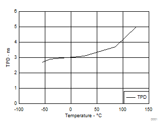
 Figure 1. TPD Across Temperature
 at 3.3 V VCC
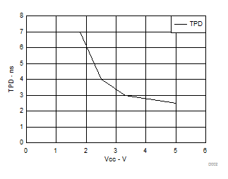
 Figure 2. TPD Across VCC at 25°C
7 Parameter Measurement Information
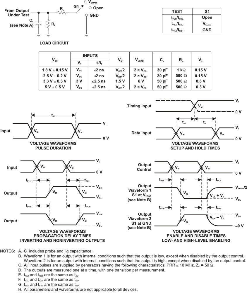
 Figure 3. Load Circuit and Voltage Waveforms
 Figure 4. Load Circuit and Voltage Waveforms
8 Detailed Description
8.1 Overview
The SN74LVC1G32 device contains one 2-input positive OR gate device and performs the Boolean function  . This device is fully specified for partial-power-down applications using Ioff. The Ioff circuitry disables the outputs, preventing damaging current backflow through the device when it is powered down.
The DPW package technology is a major breakthrough in IC packaging. Its tiny 0.64 mm square footprint saves significant board space over other package options while still retaining the traditional manufacturing friendly lead pitch of 0.5 mm.
8.2 Functional Block Diagram

8.3 Feature Description
- Wide operating voltage range.
- Operates from 1.65 V to 5.5 V.
- Allows down voltage translation.
- Inputs accept voltages to 5.5 V.
- Ioff feature allows voltages on the inputs and outputs, when VCC is 0 V.
8.4 Device Functional Modes
Function Table
| INPUTS | OUTPUT Y |
|
|---|---|---|
| A | B | |
| H | X | H |
| X | H | H |
| L | L | L |
