SCES581D JULY 2004 – October 2015 SN74LVC1GX04
UNLESS OTHERWISE NOTED, this document contains PRODUCTION DATA.
- 1 Features
- 2 Applications
- 3 Description
- 4 Revision History
- 5 Pin Configuration and Functions
-
6 Specifications
- 6.1 Absolute Maximum Ratings
- 6.2 ESD Ratings
- 6.3 Recommended Operating Conditions
- 6.4 Thermal Information
- 6.5 Electrical Characteristics
- 6.6 Switching Characteristics, SN74LVC1GX04
- 6.7 Switching Characteristics, SN74LVC1GX04
- 6.8 Switching Characteristics, SN74LVC1GX04
- 6.9 Operating Characteristics
- 6.10 Typical Characteristics
- 7 Parameter Measurement Information
- 8 Detailed Description
- 9 Application and Implementation
- 10Power Supply Recommendations
- 11Layout
- 12Device and Documentation Support
- 13Mechanical, Packaging, and Orderable Information
封装选项
请参考 PDF 数据表获取器件具体的封装图。
机械数据 (封装 | 引脚)
- DBV|6
- DRL|6
- DCK|6
散热焊盘机械数据 (封装 | 引脚)
订购信息
1 Features
- Available in Texas Instruments NanoStar™ and NanoFree™ Packages
- Supports 5-V VCC Operation
- Inputs Accept Voltages to 5.5 V
- One Unbuffered Inverter (SN74LVC1GU04) and One Buffered Inverter (SN74LVC1G04)
- Suitable for Commonly Used Clock Frequencies:
- 15 kHz, 3.58 MHz, 4.43 MHz, 13 MHz,
25 MHz, 26 MHz, 27 MHz, 28 MHz
- 15 kHz, 3.58 MHz, 4.43 MHz, 13 MHz,
- Maximum tpd of 2.4 ns at 3.3 V
- Low Power Consumption, 10-μA Maximum ICC
- ±24-mA Output Drive at 3.3 V
- Ioff Supports Partial-Power-Down Mode Operation
- Latch-Up Performance Exceeds 100 mA Per JESD 78, Class II
- ESD Protection Exceeds JESD 22
- 2000-V Human Body Model (A114-A)
- 1000-V Charged-Device Model (C101)
2 Applications
- Crystal Oscillators
- Clock Generation
3 Description
The SN74LVC1GX04 device is designed for 1.65-V to 5.5-V VCC operation. This device incorporates the SN74LVC1GU04 (inverter with unbuffered output) and the SN74LVC1G04 (inverter) functions into a single device. The LVC1GX04 is optimized for use in crystal oscillator applications.
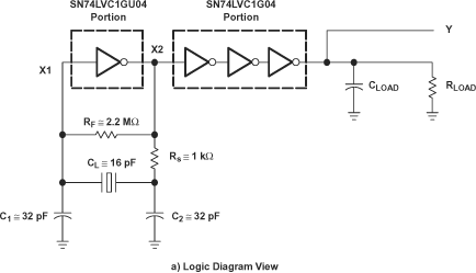
X1 and X2 can be connected to a crystal or resonator in oscillator applications. The device provides an additional buffered inverter (Y) for signal conditioning (see Figure 5). The additional buffered inverter improves the signal quality of the crystal oscillator output by making it rail to rail.
NanoStar and NanoFree package technology is a major breakthrough in IC packaging concepts, using the die as the package.
This device is fully specified for partial-power-down applications using Ioff (Y output only). The Ioff circuitry disables the outputs, preventing damaging current backflow through the device when it is powered down.
Device Information(1)
| PART NUMBER | PACKAGE | BODY SIZE (NOM) |
|---|---|---|
| SN74LVC1GX04DBV | SOT-23 (6) | 2.90 mm × 1.60 mm |
| SN74LVC1GX04DCK | SC70 (6) | 2.00 mm × 1.25 mm |
| SN74LVC1GX04DRL | SOT (6) | 1.60 mm × 1.20 mm |
Functional Block Diagram
