-
THS4281 Very Low-Power, High-Speed, Rail-to-Rail Input and Output Voltage-Feedback Operational Amplifier
- 1 Features
- 2 Applications
- 3 Description
- 4 Revision History
- 5 Pin Configuration and Functions
-
6 Specifications
- 6.1 Absolute Maximum Ratings
- 6.2 ESD Ratings
- 6.3 Recommended Operating Conditions
- 6.4 Thermal Information
- 6.5 Electrical Characteristics, VS = 3 V (VS+ = 3 V, VS- = GND)
- 6.6 Electrical Characteristics, VS = 5 V (VS+ = 5 V, VS- = GND)
- 6.7 Electrical Characteristics, VS = ±5 V
- 6.8 Dissipation Ratings
- 6.9 Typical Characteristics
- 7 Detailed Description
- 8 Application and Implementation
- 9 Power Supply Recommendations
- 10Layout
- 11Device and Documentation Support
- 12Mechanical, Packaging, and Orderable Information
- IMPORTANT NOTICE
封装选项
请参考 PDF 数据表获取器件具体的封装图。
机械数据 (封装 | 引脚)
- D|8
- DBV|5
- DGK|8
散热焊盘机械数据 (封装 | 引脚)
订购信息
THS4281 Very Low-Power, High-Speed, Rail-to-Rail Input and Output Voltage-Feedback Operational Amplifier
1 Features
- Very Low Quiescent Current: 750 μA (at 5 V)
- Rail-to-Rail Input and Output:
- Common-Mode Input Voltage Extends
400 mV Beyond the Rails - Output Swings Within 150 mV From the Rails
- Common-Mode Input Voltage Extends
- Wide –3-dB Bandwidth at 5 V:
- 90 MHz at Gain = +1, 40 MHz at Gain = +2
- High Slew Rate: 35 V/μs
- Fast Settling Time (2-V Step):
- 78 ns to 0.1%
- 150 ns to 0.01%
- Low Distortion at Gain = +2, VO = 2-VPP, 5 V:
- –91 dBc at 100 kHz, –67 dBc at 1 MHz
- Input Offset Voltage: 2.5 mV (Max at +25°C)
- Output Current > 30 mA (10-Ω Load, 5 V)
- Low Voltage Noise of 12.5 nV/√Hz
- Supply Voltages: +2.7 V, 3 V, +5 V, ±5 V, +15 V
- Packages: SOT23, MSOP, and SOIC
2 Applications
- Portable/Battery-Powered Applications
- High Channel Count Systems
- ADC Buffer
- Active Filters
- Current Sensing
3 Description
Fabricated using the BiCom-II process, the THS4281 is a low-power, rail-to-rail input and output, voltage-feedback operational amplifier designed to operate over a wide power-supply range of 2.7-V to 15-V single supply, and ±1.35-V to ±7.5-V dual supply. Consuming only 750 μA with a unity gain bandwidth of 90 MHz and a high 35-V/μs slew rate, the THS4281 allows portable or other power-sensitive applications to realize high performance with minimal power. To ensure long battery life in portable applications, the quiescent current is trimmed to be less than 900 μA at +25°C, and 1 mA from –40°C to +85°C.
The THS4281 is a true single-supply amplifier with a specified common-mode input range of 400 mV beyond the rails. This allows for high-side current sensing applications without phase reversal concerns. Its output swings to within 40 mV from the rails with 10-kΩ loads, and 150 mV from the rails with 1-kΩ loads.
The THS4281 has a good 0.1% settling time of 78 ns, and 0.01% settling time of 150 ns. The low THD of –87 dBc at 100 kHz, coupled with a maximum offset voltage of less than 2.5 mV, makes the THS4281 a good match for high-resolution ADCs sampling less than 2 MSPS.
The THS4281 is offered in a space-saving SOT23-5 package, a small MSOP-8 package, and the industry standard SOIC-8 package.
Device Information(1)
| PART NUMBER | PACKAGE | BODY SIZE (NOM) |
|---|---|---|
| THS4281 | SOIC (8) | 4.90 mm × 3.91 mm |
| SOT-23 (5) | 2.90 mm × 1.60 mm | |
| VSSOP (8) | 3.00 mm × 3.00 mm |
- For all available packages, see the orderable addendum at the end of the data sheet.
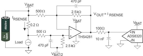
High-side, Low Power Current-Sensing system

4 Revision History
Changes from A Revision (November 2009) to B Revision
- Added Pin Configuration and Functions section, ESD Ratings table, Feature Description section, Device Functional Modes, Application and Implementation section, Power Supply Recommendations section, Layout section, Device and Documentation Support section, and Mechanical, Packaging, and Orderable Information section Go
- Removed the Packaging/Ordering Information table Go
- Removed Design Tools section Go
- Updated Thermal Values Go
- Removed the Applications Section Contents section Go
- Removed the Bill of Materials section Go
Changes from * Revision (April 2004) to A Revision
- Updated document format to current standardsGo
- Deleted Lead temperature specification from Absolute Maximum Ratings tableGo
- Revised Driving Capacitive Loads sectionGo
- Changed Board Layout section; revised statements in fourth recommendation about how to make connections to other wideband devices on the boardGo