SLAS538B October 2007 – November 2016 TLV320AIC34
PRODUCTION DATA.
- 1 Features
- 2 Applications
- 3 Description
- 4 Revision History
- 5 Description (continued)
- 6 Device Comparison Table
- 7 Pin Configuration and Functions
- 8 Specifications
-
9 Detailed Description
- 9.1 Overview
- 9.2 Functional Block Diagram
- 9.3
Feature Description
- 9.3.1 Hardware Reset
- 9.3.2 I2C Bus Debug In A Glitched System
- 9.3.3 Digital Audio Data Serial Interface
- 9.3.4 TDM Data Transfer
- 9.3.5 Audio Data Converters
- 9.3.6 Audio Clock Generation
- 9.3.7 Stereo Audio ADC
- 9.3.8 Digital Audio Processing For Record Path
- 9.3.9 Automatic Gain Control (AGC)
- 9.3.10 Stereo Audio DAC
- 9.3.11 Digital Audio Processing For Playback
- 9.3.12 Digital Interpolation Filter
- 9.3.13 Delta-Sigma Audio DAC
- 9.3.14 Audio DAC Digital Volume Control
- 9.3.15 Increasing DAC Dynamic Range
- 9.3.16 Analog Output Common-Mode Adjustment
- 9.3.17 Audio DAC Power Control
- 9.3.18 Audio Analog Inputs
- 9.3.19 Analog Input Bypass Path Functionality
- 9.3.20 ADC PGA Signal Bypass Path Functionality
- 9.3.21 Input Impedance and VCM Control
- 9.3.22 Passive Analog Bypass During Power Down
- 9.3.23 MICBIAS_x Generation
- 9.3.24 Digital Microphone Connectivity
- 9.3.25 Analog Fully Differential Line Output Drivers
- 9.3.26 Analog High-Power Output Drivers
- 9.3.27 Short-Circuit Output Protection
- 9.3.28 Jack or Headset Detection
- 9.3.29 Output Stage Volume Controls
- 9.4 Device Functional Modes
- 9.5 Programming
- 9.6 Register Maps
- 10Application and Implementation
- 11Power Supply Recommendations
- 12Layout
- 13Device and Documentation Support
- 14Mechanical, Packaging, and Orderable Information
1 Features
- Four-Channel Audio DAC
- 102-dBA Signal-to-Noise Ratio
- 16-, 20-, 24-, and 32-Bit Data
- Supports Rates From 8 kHz to 96 kHz
- 3D, Bass, Treble, EQ, and De-Emphasis Effects
- Flexible Power Saving Modes and Performance Are Available
- Four-Channel Audio ADC
- 92-dBA Signal-to-Noise Ratio
- Supports Rates From 8 kHz to 96 kHz
- Digital Signal Processing and Noise Filtering Available During Record
- Twelve Audio Inputs
- Programmable in Single-Ended or Fully Differential Configurations
- 3-State Capability for Floating Input Configurations
- Fourteen Audio Output Drivers
- Stereo 8-Ω, 500-mW/Channel Speaker Drive Capability
- Multiple Fully Differential or Single-Ended Headphone Drivers
- Multiple Fully Differential or Single-Ended Line Outputs
- Fully Differential Mono Outputs
- Low Power: 15-mW Stereo 48-kHz Playback With 3.3-V Analog Supply
- Ultra-Low-Power Mode With Passive Analog Bypass
- Programmable Input/Output Analog Gains
- Automatic Gain Control (AGC) for Record
- Programmable Microphone Bias Level
- Dual Programmable PLLs for Flexible Clock Generation
- I2C Control Bus
- Dual Audio Serial Data Busses
- Support I2S, Left- or Right-Justified, DSP, PCM, and TDM Modes
- Enable Asynchronous Simultaneous Operation of Busses and Data Converters
- Digital Microphone Input Support
- Concurrent Digital Microphone and Analog Microphone Support Available
- Extensive Modular Power Control
- Power Supplies:
- Analog: 2.7 V to 3.6 V
- Digital Core: 1.65 V to 1.95 V
- Digital I/O: 1.1 V to 3.6 V
- Package: 6-mm × 6-mm 87-pin NFBGA
2 Applications
- Digital Cameras
- Smart Cellular Phones
3 Description
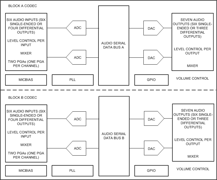
The TLV320AIC34 device is a low-power four-channel audio codec with four-channel headphone amplifier, as well as multiple inputs and outputs programmable in single-ended or fully differential configurations. Extensive register-based power control is included, enabling four-channel 48-kHz DAC playback as low as 15 mW from a 3.3-V analog supply, making it ideal for portable battery-powered audio and telephony applications.
Device Information(1)
| PART NUMBER | PACKAGE | BODY SIZE (NOM) |
|---|---|---|
| TLV320AIC34 | NFBGA (87) | 6.00 mm × 6.00 mm |
- For all available packages, see the orderable addendum at the end of the data sheet.
Block A and B Codec
