SLVSAC4B November   2010  – December 2015 TLV62065

PRODUCTION DATA.  

  1. Features
  2. Applications
  3. Description
  4. Revision History
  5. Pin Configuration and Functions
  6. Specifications
    1. 6.1 Absolute Maximum Ratings
    2. 6.2 ESD Ratings
    3. 6.3 Recommended Operating Conditions
    4. 6.4 Thermal Information
    5. 6.5 Electrical Characteristics
    6. 6.6 Typical Characteristics
  7. Detailed Description
    1. 7.1 Overview
    2. 7.2 Functional Block Diagram
    3. 7.3 Feature Description
      1. 7.3.1 Mode Selection
      2. 7.3.2 Enable
      3. 7.3.3 Undervoltage Lockout
      4. 7.3.4 Thermal Shutdown
    4. 7.4 Device Functional Modes
      1. 7.4.1 Soft-Start
      2. 7.4.2 Power-Save Mode
        1. 7.4.2.1 100% Duty Cycle Low Dropout Operation
      3. 7.4.3 Internal Current Limit / Fold-back Current Limit for Short-Circuit Protection
      4. 7.4.4 Output Capacitor Discharge
  8. Application and Implementation
    1. 8.1 Application Information
    2. 8.2 Typical Application
      1. 8.2.1 Design Requirements
      2. 8.2.2 Detailed Design Procedure
        1. 8.2.2.1 Output Voltage Setting
        2. 8.2.2.2 Output Filter Design (Inductor and Output Capacitor)
          1. 8.2.2.2.1 Inductor Selection
          2. 8.2.2.2.2 Output Capacitor Selection
          3. 8.2.2.2.3 Input Capacitor Selection
        3. 8.2.2.3 Checking Loop Stability
      3. 8.2.3 Application Curves
  9. Power Supply Recommendations
  10. 10Layout
    1. 10.1 Layout Guidelines
    2. 10.2 Layout Example
  11. 11Device and Documentation Support
    1. 11.1 Device Support
      1. 11.1.1 Third-Party Products Disclaimer
    2. 11.2 Community Resources
    3. 11.3 Trademarks
    4. 11.4 Electrostatic Discharge Caution
    5. 11.5 Glossary
  12. 12Mechanical, Packaging, and Orderable Information

封装选项

机械数据 (封装 | 引脚)
散热焊盘机械数据 (封装 | 引脚)
订购信息

1 Features

  • VIN Range from 2.9 V to 5.5 V
  • Up to 97% Efficiency
  • Power-Save Mode / 3-MHz Fixed PWM Mode
  • Output Voltage Accuracy in PWM Mode ±2.0%
  • Output Capacitor Discharge Function
  • Typical 18-µA Quiescent Current
  • 100% Duty Cycle for Lowest Dropout
  • Available in a 2 mm × 2 mm × 0.75 mm WSON

2 Applications

  • Point-of-Load (POL)
  • Notebooks, Pocket PCs
  • Portable Media Players
  • Set-Top Boxes

3 Description

The TLV62065 device is a high efficiency synchronous step-down DC–DC converter. It provides up to 2-A output current.

With an input voltage range of 2.9 V to 5.5 V, the device is a perfect fit for power conversion from a 5-V or 3.3-V system supply rail. The TLV62065 operates at 3-MHz fixed frequency and enters power-save mode operation at light load currents to maintain high efficiency over the entire load current range. For low noise applications, TLV62065 can be forced into fixed frequency PWM mode by pulling the MODE pin high.

In the shutdown mode, the current consumption is reduced to less than 1 µA and an internal circuit discharges the output capacitor.

TLV62065 operates with a 1-µH inductor and 10-µF output capacitor.

The TLV62065 is available in a small 2 mm × 2 mm × 0.75 mm 8-pin WSON package.

Device Information(1)

PART NUMBER PACKAGE BODY SIZE (NOM)
SLVSAC4 WSON (8) 2.00 mm × 2.00 mm
  1. For all available packages, see the orderable addendum at the end of the data sheet.

Space

Typical Application Schematic
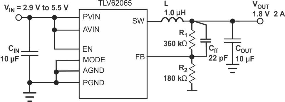
TLV62065 FP_app_eff_lvsac4.gif

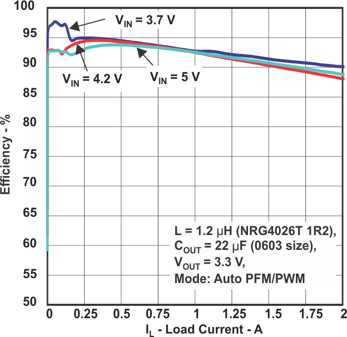
Efficiency vs Load Current

TLV62065 eff_v_load_graph.gif