SLRS066D January 2014 – March 2016 TPL7407L
PRODUCTION DATA.
- 1 Features
- 2 Applications
- 3 Description
- 4 Revision History
- 5 Pin Configuration and Functions
- 6 Specifications
- 7 Detailed Description
- 8 Application and Implementation
- 9 Power Supply Recommendations
- 10Layout
- 11Device and Documentation Support
- 12Mechanical, Packaging, and Orderable Information
1 Features
- 600-mA Rated Drain Current (Per Channel)
- CMOS Pin-to-Pin Improvement of 7-channel Darlington Array (e.g. ULN2003A)
- Power Efficient (Very low VOL)
- Less Than 4 Times Lower VOL at 100 mA Than Darlington Array
- Very Low Output Leakage < 10 nA Per Channel
- Extended Ambient Temperature Range:
TA = –40°C to 125°C - High-Voltage Outputs 40 V
- Compatible with 1.8-V to 5.0-V Micro-controllers and Logic Interface
- Internal Free-wheeling Diodes for Inductive Kick-back Protection
- Input Pull-down Resistors Allows Tri-stating the Input Driver
- Input RC-Snubber to Eliminate Spurious Operation in Noisy Environment
- Inductive Load Driver Applications
- ESD Protection Exceeds JESD 22
- 2-kV HBM, 500-V CDM
- Available in 16-pin SOIC and TSSOP Packages
2 Applications
- Inductive Loads
- Relays
- Unipolar Stepper & Brushed DC Motors
- Solenoids & Valves
- LEDs
- Logic Level Shifting
- Gate & IGBT Drive
3 Description
The TPL7407L is a high-voltage, high-current NMOS transistor array. This device consists of seven NMOS transistors that feature high-voltage outputs with common-cathode clamp diodes for switching inductive loads. The maximum drain-current rating of a single NMOS channel is 600 mA. New regulation and drive circuitry added to give maximum drive strength across all GPIO ranges (1.8 V – 5.0 V).The transistors can be paralleled for higher current capability.
The TPL7407L's key benefit is its improved power efficiency and lower leakage than a Bipolar Darlington Implementation. With the lower VOL the user is dissipating less than half the power than traditional relay drivers with currents less than 250 mA per channel.
Device Information(1)
| PART NUMBER | PACKAGE (PINS) | BODY SIZE (NOM) |
|---|---|---|
| TPL7407LD | SOIC (16) | 9.90 mm x 3.91 mm |
| TPL7407LPW | TSSOP (16) | 5.00 mm x 4.40 mm |
- For all available packages, see the orderable addendum at the end of the datasheet.
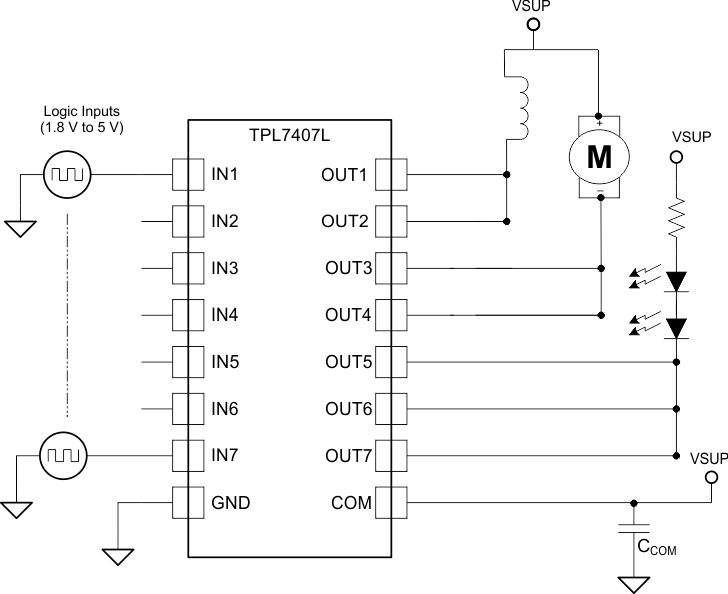
Simple Application Schematic
