SLVSA01C May 2011 – June 2016 TPS2062-Q1 , TPS2065-Q1
PRODUCTION DATA.
- 1 Features
- 2 Applications
- 3 Description
- 4 Revision History
- 5 Pin Configuration and Functions
- 6 Specifications
- 7 Parameter Measurement Information
- 8 Detailed Description
-
9 Application and Implementation
- 9.1
Application Information
- 9.1.1 Overcurrent
- 9.1.2 OC Response
- 9.1.3 Undervoltage Lockout (UVLO)
- 9.1.4 Universal Serial Bus (USB) Applications
- 9.1.5 Host, Self-Powered (SPH), and Bus-Powered Hubs (BPH)
- 9.1.6 Low-Power Bus-Powered and High-Power Bus-Powered Functions
- 9.1.7 USB Power-Distribution Requirements
- 9.1.8 Generic Hot-Plug Applications
- 9.2 Typical Application
- 9.1
Application Information
- 10Power Supply Recommendations
- 11Layout
- 12Device and Documentation Support
- 13Mechanical, Packaging, and Orderable Information
1 Features
- Qualified for Automotive Applications
- 70-mΩ High-Side MOSFET
- 1-A Continuous Current
- Thermal and Short-Circuit Protection
- Accurate Current Limit
(1.1-A Minimum, 2.1-A Maximum) - Operating Range: 2.7 V to 5.5 V
- 0.6-ms Typical Rise Time
- Undervoltage Lockout
- Deglitched Fault Report (OC)
- No OC Glitch During Power Up
- 1-μA Maximum Standby Supply Current
- Bidirectional Switch
- Built-in Soft Start
- UL Recognized Under File No. E166910
- Ambient Temperature Range: –40°C to 125°C
3 Description
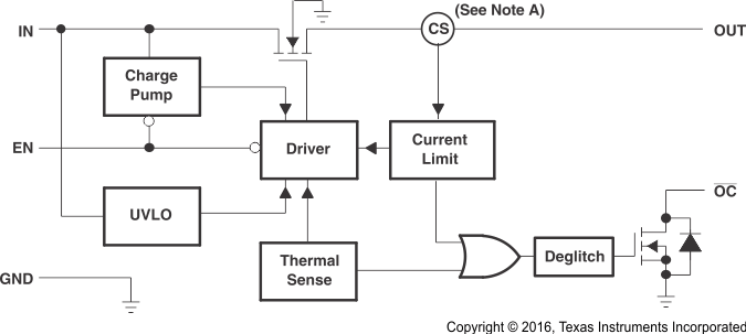
The TPS206x-Q1 power-distribution switch is intended for applications where heavy capacitive loads and short circuits are likely to be encountered. This device incorporates 70-mΩ N-channel MOSFET power switches for power-distribution systems that require multiple power switches in a single package. Each switch is controlled by a logic enable input. Gate drive is provided by an internal charge pump designed to control the power-switch rise times and fall times to minimize current surges during switching. The charge pump requires no external components and allows operation from supplies as low as 2.7 V.
When the output load exceeds the current-limit threshold or a short is present, the device limits the output current to a safe level by switching into a constant-current mode, pulling the overcurrent (OCx) logic output low. When continuous heavy overloads and short circuits increase the power dissipation in the switch, causing the junction temperature to rise, a thermal protection circuit shuts off the switch to prevent damage. Recovery from a thermal shutdown is automatic once the device has cooled sufficiently. Internal circuitry ensures that the switch remains off until valid input voltage is present. This power-distribution switch is designed to set current limit at 1.5 A (typically).
Device Information(1)
| PART NUMBER | PACKAGE | BODY SIZE (NOM) |
|---|---|---|
| TPS206x-Q1 | MSOP-PowerPAD (8) | 3.00 mm × 3.00 mm |
- For all available packages, see the orderable addendum at the end of the data sheet.
TPS2065-Q1 Functional Block Diagram
