SLVS941G April 2009 – August 2016 TPS62230
PRODUCTION DATA.
- 1 Features
- 2 Applications
- 3 Description
- 4 Revision History
- 5 Device Comparison Table
- 6 Pin Configuration and Functions
- 7 Specifications
- 8 Detailed Description
-
9 Application and Implementation
- 9.1 Application Information
- 9.2
Typical Application
- 9.2.1 Design Requirements
- 9.2.2 Detailed Design Procedure
- 9.2.3
Application Curves
- 9.2.3.1 VOUT = 1.1 V - TPS622311
- 9.2.3.2 VOUT = 1.2 V - TPS62232/TPS62235
- 9.2.3.3 VOUT = 1.8 V - TPS62231
- 9.2.3.4 VOUT = 1.85 V - TPS62236
- 9.2.3.5 VOUT = 2.5 V - TPS62230
- 9.2.3.6 VOUT = 3.0 V - TPS62233
- 9.2.3.7 Start-Up
- 9.2.3.8 PFM / PWM Operation
- 9.2.3.9 Peak-to-Peak Output Ripple Voltage
- 9.2.3.10 Power-Supply Rejection
- 9.2.3.11 Spurious Output Noise
- 9.2.3.12 Line Transient Response
- 9.2.3.13 Mode Transition
- 9.2.3.14 AC-Load Regulation
- 9.2.3.15 Load Transient Response
- 9.3 System Examples
- 10Power Supply Recommendations
- 11Layout
- 12Device and Documentation Support
- 13Mechanical, Packaging, and Orderable Information
1 Features
- 2 MHz / 3 MHz Switching Frequency
- Up to 94% Efficiency
- Output Peak Current up to 500 mA
- Operating Junction Temperature of –40°C to 125°C
- High PSRR (up to 90 dB)
- Small External Output Filter Components 1 μH and 4.7 μF
- VIN range from 2.05 V to 6 V
- Optimized Power-Save Mode for Low Output Ripple Voltage
- Forced PWM Mode Operation
- Typ. 22-μA Quiescent Current
- 100% Duty Cycle for Lowest Dropout
- Small 1-mm × 1.5-mm × 0.6-mm USON Package
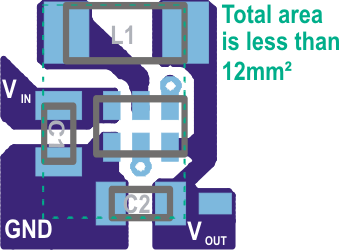
- 12-mm2 Minimum Solution Size
- Supports 0.6-mm Maximum Solution Height
2 Applications
- LDO Replacement
- Portable Audio, Portable Media
- Low Power Wireless
- Low Power DSP Core Supply
- Digital Cameras
3 Description
The TPS6223x device family is a high-frequency, synchronous, step-down DC – DC converter optimized for battery powered portable applications. It supports up to 500-mA output current and allows the use of tiny and low-cost chip inductors and capacitors.
With a wide input voltage range of 2.05 V to 6 V, the device supports applications powered by Li-Ion batteries with extended voltage range. The minimum input voltage of 2.05 V allows as well the operation from Li-primary or two alkaline batteries. Different fixed output voltage versions are available from 1.0 V to 3.3 V.
The TPS6223x series features switch frequency up to 3.8 MHz. At medium to heavy loads, the converter operates in pulse width modulation (PWM) mode and automatically enters power-save mode operation at light load currents to maintain high efficiency over the entire load current range.
Because of its excellent power supply rejection ratio (PSRR) and AC load regulation performance, the device is also suitable to replace linear regulators to obtain better power conversion efficiency.
The power-save mode in TPS6223x reduces the quiescent current consumption down to 22 μA during light load operation. It is optimized to achieve very low output voltage ripple even with small external component and features excellent AC load regulation.
For very noise-sensitive applications, the device can be forced to PWM mode operation over the entire load range by pulling the MODE pin high. In the shutdown mode, the current consumption is reduced to less than 1 μA. The TPS6223x operates over a junction temperature range of –40°C to 125°C. It is available in a 1 mm × 1.5 mm × 0.6 mm 6-pin SON package.
Device Information(1)
| PART NUMBER | PACKAGE | BODY SIZE (NOM) |
|---|---|---|
| TPS6223xx | USON (6) | 1.45 mm x 1.00 mm |
- For all available packages, see the orderable addendum at the end of the data sheet.
Typical Application Schematic

Small PCB Layout Size
