SLWS230E September   2011  – December 2015 TRF3765

PRODUCTION DATA.  

  1. Features
  2. Applications
  3. Description
  4. Revision History
  5. Pin Configuration and Functions
  6. Specifications
    1. 6.1 Absolute Maximum Ratings
    2. 6.2 ESD Ratings
    3. 6.3 Recommended Operating Conditions
    4. 6.4 Thermal Information
    5. 6.5 Electrical Characteristics
    6. 6.6 4WI Timing: Write Operation
    7. 6.7 Readback 4WI Timing
    8. 6.8 Typical Characteristics
  7. Detailed Description
    1. 7.1 Overview
    2. 7.2 Functional Block Diagram
    3. 7.3 Feature Description
      1. 7.3.1 Lock Detect
      2. 7.3.2 LO Divider
      3. 7.3.3 Selecting the VCO and VCO Frequency Control
      4. 7.3.4 External VCO
    4. 7.4 Device Functional Modes
      1. 7.4.1 VCO_TEST_MODE
      2. 7.4.2 Readback Mode
      3. 7.4.3 Integer and Fractional Mode Selection
      4. 7.4.4 PLL Architecture
        1. 7.4.4.1 Selecting PLL Divider Values
        2. 7.4.4.2 Setup Example for Integer Mode
        3. 7.4.4.3 Setup Example for Fractional Mode
      5. 7.4.5 Fractional Mode Setup
    5. 7.5 Register Maps
      1. 7.5.1 PLL 4WI Registers
        1. 7.5.1.1 Register 1
          1. 7.5.1.1.1 CAL_CLK_SEL[3..0]
          2. 7.5.1.1.2 ICP[4..0]
        2. 7.5.1.2 Register 2
          1. 7.5.1.2.1 PLL_DIV <1.0>
          2. 7.5.1.2.2 VCOSEL_MODE
        3. 7.5.1.3 Register 3
        4. 7.5.1.4 Register 4
        5. 7.5.1.5 Register 5
        6. 7.5.1.6 Register 6
      2. 7.5.2 Readback from the Internal Register Banks
        1. 7.5.2.1 Register 0 Write
          1. 7.5.2.1.1 Register 0 Read
  8. Application and Implementation
    1. 8.1 Application Information
    2. 8.2 Typical Application
      1. 8.2.1 Design Requirements
      2. 8.2.2 Detailed Design Procedures
        1. 8.2.2.1 Power Supply
        2. 8.2.2.2 Loop Filter
        3. 8.2.2.3 Reference Clock
      3. 8.2.3 Application Curves
  9. Power Supply Recommendations
  10. 10Layout
    1. 10.1 Layout Guidelines
    2. 10.2 Layout Example
  11. 11Device and Documentation Support
    1. 11.1 Trademarks
    2. 11.2 Electrostatic Discharge Caution
    3. 11.3 Glossary
  12. 12Mechanical, Packaging, and Orderable Information

封装选项

机械数据 (封装 | 引脚)
散热焊盘机械数据 (封装 | 引脚)
订购信息

1 Features

  • Output Frequencies: 300 MHz to 4.8 GHz
  • Low-Noise VCO: –133 dBc/Hz
    (1-MHz Offset, fOUT = 2.65 GHz)
  • 13-/16-Bit Reference/Feedback Divider
  • 25-Bit Fractional-N and Integer-N PLL
  • Low RMS Jitter: 0.35 ps
  • Input Reference Frequency Range:
    0.5 MHz to 350 MHz
  • Programmable Output Divide-by-1/-2/-4/-8
  • Four Differential LO Outputs
  • External VCO Input with Programmable VCO On/Off Control

2 Applications

  • Wireless Infrastructure
  • Wireless Local Loop
  • Point-to-Point Wireless Access
  • Wireless MAN Wideband Transceivers

3 Description

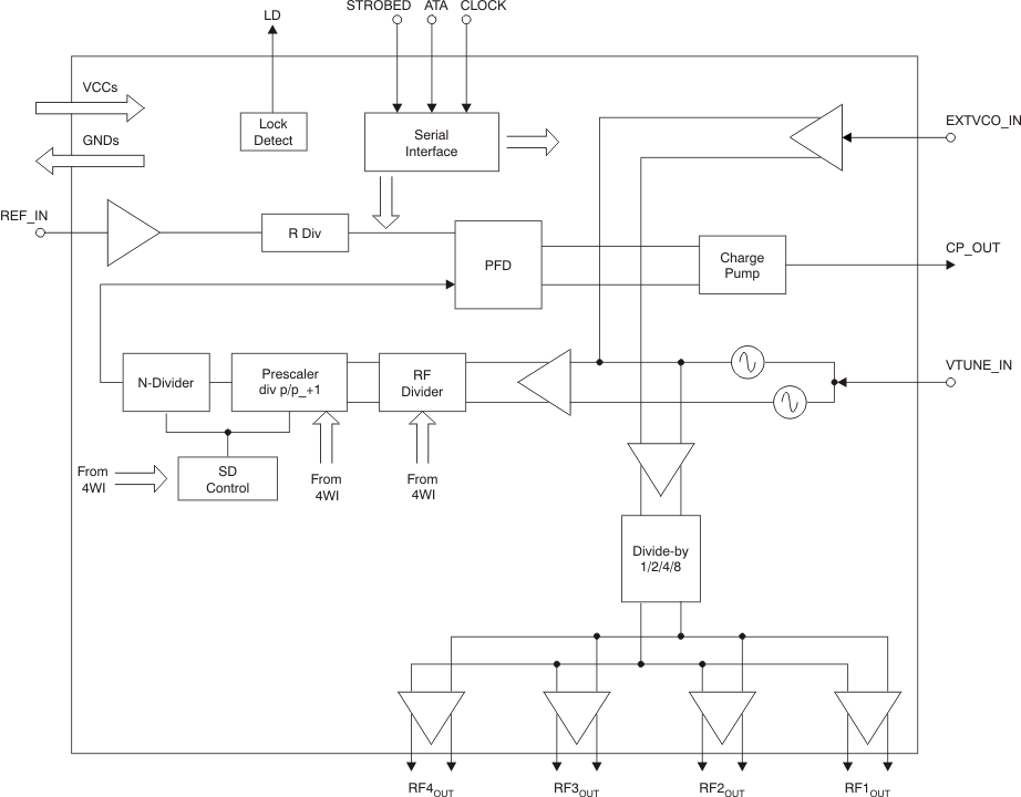
The TRF3765 is a wideband Integer-N/Fractional-N frequency synthesizer with an integrated, wideband voltage-controlled oscillator (VCO). Programmable output dividers enable continuous frequency coverage from 300 MHz to 4.8 GHz. Four separate differential, open-collector RF outputs allow multiple devices to be driven in parallel without the need of external splitters.

The TRF3765 also accepts external VCO input signals and allows on/off control through a programmable control output. For maximum flexibility and wide reference frequency range, wide-range divide ratio settings are programmable and an off-chip loop filter can be used.

The TRF3765 is available in an RHB-32 VQFN package.

Device Information(1)

PART NUMBER PACKAGE BODY SIZE (NOM)
TRF3765 VQFN (32) 5.00 mm x 5.00 mm
  1. For all available packages, see the orderable addendum at the end of the datasheet.

Block Diagram
TRF3765 fbd_lws230.gif