SCES638D October 2007 – June 2017 TXS0101
PRODUCTION DATA.
- 1 Features
- 2 Applications
- 3 Description
- 4 Revision History
- 5 Pin Configuration and Functions
-
6 Specifications
- 6.1 Absolute Maximum Ratings
- 6.2 ESD Ratings
- 6.3 Recommended Operating Conditions
- 6.4 Thermal Information
- 6.5 Electrical Characteristics
- 6.6 Timing Requirements: V CCA = 1.8 V ± 0.15 V
- 6.7 Timing Requirements VCCA = 2.5 V ± 0.2 V
- 6.8 Timing Requirements: 3.3 V ± 0.3 V
- 6.9 Switching Characteristics: VCCA = 1.8 V ± 0.15 V
- 6.10 Switching Characteristics: VCCA = 2.5 V ± 0.2 V
- 6.11 Switching Characteristics: VCCA = 3.3 V ± 0.3 V
- 6.12 Typical Characteristics
- 7 Parameter Measurement Information
- 8 Detailed Description
- 9 Application and Implementation
- 10Power Supply Recommendations
- 11Layout
- 12Device and Documentation Support
- 13Mechanical, Packaging, and Orderable Information
封装选项
机械数据 (封装 | 引脚)
散热焊盘机械数据 (封装 | 引脚)
订购信息
1 Features
- Latch-Up Performance Exceeds 100 mA Per JESD 78, Class II
- ESD Protection Exceeds JESD 22
- A Port
- 2500 V Human-Body Model (A114-B)
- 200 V Machine Model (A115-A)
- 1500 V Charged-Device Model (C101)
- B Port
- 8 kV Human-Body Model (A114-B)
- 200 V Machine Model (A115-A)
- 1500 V Charged-Device Model (C101)
- A Port
- No Direction-Control Signal Needed
- Maximum Data Rates
- 24 Mbps (Push Pull)
- 2 Mbps (Open Drain)
- Available in the Texas Instruments NanoFree™ Package
- 1.65 V to 3.6 V on A port and 2.3 V to 5.5 V on B port (VCCA ≤ VCCB)
- VCC Isolation Feature – If Either VCC Input Is at GND, Both Ports Are in the High-Impedance State
- No Power-Supply Sequencing Required – Either VCCA or VCCB Can be Ramped First
- Ioff Supports Partial-Power-Down Mode Operation
2 Applications
- Handsets
- Smartphones
- Tablets
- Desktop PCs
3 Description
This one-bit non-inverting translator uses two separate configurable power-supply rails. The A port is designed to track VCCA. VCCA accepts any supply voltage from 1.65 V to 3.6 V. The B port is designed to track VCCB. VCCA must be less than or equal to VCCB. VCCB accepts any supply voltage from 2.3 V to 5.5 V. This allows for low voltage bidirectional translation between any of the 1.8 V, 2.5 V, 3.3 V, and 5 V voltage nodes.
When the output-enable (OE) input is low, all outputs are placed in the high-impedance state.
To ensure the high-impedance state during power up or power down, OE should be tied to GND through a pull-down resistor; the minimum value of the resistor is determined by the current-sourcing capability of the driver.
Device Information(1)
| PART NUMBER | PACKAGE | BODY SIZE (NOM) |
|---|---|---|
| TXS0101DBV | SOT-23 (6) | 2.90 mm × 1.60 mm |
| TXS0101DCK | SC70 (6) | 2.00 mm × 1.25 mm |
| TXS0101DRL | SOT-5X3 (6) | 1.90 mm × 1.60 mm |
| TXS0101YZP | DSBGA (6) | 0.89 mm × 1.39 mm |
- For all available packages, see the orderable addendum at the end of the data sheet.
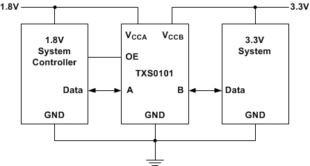
Typical Operating Circuit
