SGLS378G March 2008 – October 2017 ADS5463-SP
PRODUCTION DATA.
- 1 Features
- 2 Applications
- 3 Description
- 4 Revision History
- 5 Pin Configuration and Functions
-
6 Specifications
- 6.1 Absolute Maximum Ratings
- 6.2 ESD Ratings
- 6.3 Recommended Operating Conditions
- 6.4 Thermal Information
- 6.5 Electrical Characteristics: ADS5463-RHA
- 6.6 Electrical Characteristics: ADS5463-RHA
- 6.7 Electrical Characteristics: ADS5463-RHA
- 6.8 Electrical Characteristics: ADS5463-SP
- 6.9 Electrical Characteristics: ADS5463-SP
- 6.10 Electrical Characteristics: ADS5463-SP
- 6.11 Timing Requirements
- 6.12 Typical Characteristics
- 7 Detailed Description
- 8 Application and Implementation
- 9 Power Supply Recommendations
- 10Layout
- 11Device and Documentation Support
- 12Mechanical, Packaging, and Orderable Information
1 Features
- 500-MSPS Sample Rate
- Available With Radiation Hardness Specified (RHA) - Total Ionizing Dose 100 krad(Si), ELDRS Free 100 krad(Si)
- 12-Bit Resolution, 10-Bits Effective Number of Bits (ENOB)
- SNR > 64.5 dBFS at 450 MHz and 500 MSPS
- SFDR > 64.0 dBc at 450 MHz and 500 MSPS
- 2.2-VPP Differential Input Voltage
- LVDS-Compatible Outputs
- Total Power Dissipation: 2.2 W
- Offset Binary Output Format
- Output Data Transitions on the Rising and Falling Edges of a Half-Rate Output Clock
- On-Chip Analog Buffer, Track and Hold, and Reference Circuit
- Available in a 84-Pin Ceramic Nonconductive Tie-Bar Package (HFG)
- Military Temperature Range (–55°C to 125°C Tcase)
2 Applications
3 Description
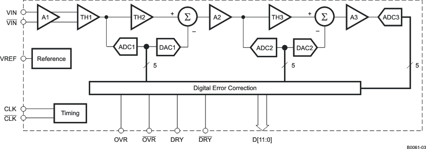
The ADS5463 is a 12-bit, 500-MSPS analog-to-digital converter (ADC) that operates from both a 5-V supply and 3.3-V supply, while providing LVDS-compatible digital outputs from the 3.3-V supply. The ADS5463 input buffer isolates the internal switching of the onboard track and hold (T and H) from disturbing the signal source. An internal reference generator is also provided to simplify the system design further. The ADS5463 has outstanding low noise and linearity over input frequency.
The ADS5463 is available in a 84-pin ceramic nonconductive tie-bar package (HFG). The ADS5463 is built on state-of-the-art Texas Instruments complementary bipolar process (BiCom3X) and is specified over the full military temperature range (–55°C to 125°C Tcase).
Device Information(2)
| PART NUMBER | PACKAGE | BODY SIZE (NOM) |
|---|---|---|
| ADS5463-SP | CFP (84) | 16.51 mm × 16.51 mm |
- These units are intended for engineering evaluation only. They are processed to a non-compliant flow (for example, no burn-in, and so forth) and are tested to temperature rating of 25°C only. These units are not suitable for qualification, production, radiation testing or flight use. Parts are not warranted for performance on full MIL specified temperature range of –55°C to 125°C or operating life.
- For all available packages, see the orderable addendum at the end of the data sheet.
Block Diagram
