SLUS900E December 2008 – August 2015
PRODUCTION DATA.
- 1 Features
- 2 Applications
- 3 Description
- 4 Revision History
- 5 Pin Configuration and Functions
- 6 Specifications
-
7 Detailed Description
- 7.1 Overview
- 7.2 Functional Block Diagram
- 7.3 Feature Description
- 7.4 Device Functional Modes
- 7.5 Programming
- 7.6
Register Maps
- 7.6.1 I2C Read After Backup Mode
- 7.6.2
Normal Register Descriptions
- 7.6.2.1 SECONDS Register (address = 0x00) [reset = 0XXXXXXb]
- 7.6.2.2 MINUTES Register (address = 0x01) [reset = 1XXXXXXb]
- 7.6.2.3 CENT_HOURS Register (address = 0x02) [reset = XXXXXXXXb]
- 7.6.2.4 DAY Register (address = 0x03) [reset = 00000XXXb]
- 7.6.2.5 DATE Register (address = 0x04) [reset = 00XXXXXXb]
- 7.6.2.6 MONTH Register (address = 0x05) [reset = 000XXXXXb]
- 7.6.2.7 YEARS Register (address = 0x06) [reset = XXXXXXXXb]
- 7.6.2.8 CAL_CFG1 Register (address = 0x07) [reset = 10000000b]
- 7.6.2.9 TCH2 Register (address = 0x08) [reset = 10010000b]
- 7.6.2.10 CFG2 Register (address = 0x09) [reset = 10101010b]
- 7.6.3 Special Function Registers
- 8 Application and Implementation
- 9 Power Supply Recommendations
- 10Layout
- 11Device and Documentation Support
- 12Mechanical, Packaging, and Orderable Information
1 Features
2 Applications
- General Consumer Electronics
3 Description
The bq32000 device is a compatible replacement for industry standard real-time clocks.
The bq32000 features an automatic backup supply with integrated trickle charger. The backup supply can be implemented using a capacitor or non-rechargeable battery. The bq32000 has a programmable calibration adjustment from –63 ppm to +126 ppm. The bq32000 registers include an OF (oscillator fail) flag indicating the status of the RTC oscillator, as well as a STOP bit that allows the host processor to disable the oscillator. The time registers are normally updated once per second, and all the registers are updated at the same time to prevent a timekeeping glitch. The bq32000 includes automatic leap-year compensation.
Device Information(1)
| PART NUMBER | PACKAGE | BODY SIZE (NOM) | |
|---|---|---|---|
| bq32000 | SOIC (8) | 4.90 mm x 3.91 mm | |
- For all available packages, see the orderable addendum at the end of the data sheet.
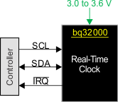
Simplified Schematic
