SCAS892C February 2010 – December 2016 CDCE937-Q1 , CDCEL937-Q1
PRODUCTION DATA.
- 1 Features
- 2 Applications
- 3 Description
- 4 Revision History
- 5 Description (continued)
- 6 Device Comparison Table
- 7 Pin Configuration and Functions
- 8 Specifications
- 9 Parameter Measurement Information
-
10Detailed Description
- 10.1 Overview
- 10.2 Functional Block Diagram
- 10.3 Feature Description
- 10.4 Device Functional Modes
- 10.5
Programming
- 10.5.1 Data Protocol
- 10.5.2 Command Code Definition
- 10.5.3 Generic Programming Sequence
- 10.5.4 Byte Write Programming Sequence
- 10.5.5 Byte Read Programming Sequence
- 10.5.6 Block Write Programming Sequence
- 10.5.7 Block Read Programming Sequence
- 10.5.8 Timing Diagram for the SDA and SCL Serial Control Interface
- 10.5.9 SDA and SCL Hardware Interface
- 10.6 Register Maps
- 11Application and Implementation
- 12Power Supply Recommendations
- 13Layout
- 14Device and Documentation Support
- 15Mechanical, Packaging, and Orderable Information
1 Features
- Qualified for Automotive Applications
- AEC-Q100 Qualified With the Following Results:
- Device Temperature Grade 1: –40°C to 125°C Ambient Operating Temperature Range
- Device HBM ESD Classification Level 2
- Device CDM ESD Classification Level C4B
- In-System Programmability and EEPROM
- Serial Programmable Volatile Register
- Nonvolatile EEPROM to Store Customer Setting
- Flexible Input Clocking Concept
- External Crystal: 8 MHz to 32 MHz
- On-Chip VCXO: Pull Range ±150 ppm
- Single-Ended LVCMOS up to 160 MHz
- Free Selectable Output Frequency up to 230 MHz
- Low-Noise PLL Core
- Integrated PLL Loop Filter Components
- Low Period Jitter (Typical 60 ps)
- Separate Output Supply Pins
- CDCE937-Q1: 3.3 V and 2.5 V
- CDCEL937-Q1: 1.8 V
- Flexible Clock Driver
- Three User-Definable Control Inputs [S0/S1/S2]; for Example: SSC Selection, Frequency Switching, Output Enable or Power Down
- Generates Highly Accurate Clocks for Video, Audio, USB, IEEE1394, RFID, Bluetooth™, WLAN, Ethernet™, and GPS
- Generates Common Clock Frequencies Used With TI-DaVinci™, OMAP™, DSPs
- Programmable SSC Modulation
- Enables 0-PPM Clock Generation
- 1.8-V Device Power Supply
- Wide Temperature Range –40°C to 125°C
- Packaged in TSSOP
- Development and Programming Kit for Easy PLL Design and Programming (TI Pro-Clock™)
3 Description
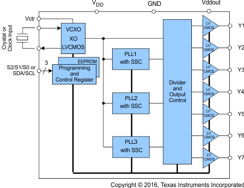
The CDCE937-Q1 and CDCEL937-Q1 devices are modular, phase-locked loop (PLL) based programmable clock synthesizers. These devices provide flexible and programmable options, such as output clocks, input signals, and control pins, so that the user can configure the CDCEx937-Q1 for their own specifications.
The CDCEx937-Q1 generates up to seven output clocks from a single input frequency to enable both board space and cost savings. Additionally, with multiple outputs, the clock generator can replace multiple crystals with one clock generator. This makes the device well-suited for head unit and telematics applications in infotainment and camera systems in ADAS as these platforms are evolving into smaller and more cost effective systems.
Device Information(1)
| PART NUMBER | PACKAGE | BODY SIZE (NOM) |
|---|---|---|
| CDCE937-Q1, CDCEL937-Q1 |
TSSOP (20) | 6.50 mm × 4.40 mm |
- For all available packages, see the orderable addendum at the end of the data sheet.
Simplified Block Diagram
