-
DAC084S085 8-Bit Micropower QUAD Digital-to-Analog Converter With Rail-to-Rail Output
- 1 Features
- 2 Applications
- 3 Description
- 4 Revision History
- 5 Description
- 6 Pin Configuration and Functions
- 7 Specifications
- 8 Detailed Description
- 9 Application and Implementation
- 10Power Supply Recommendations
- 11Layout
- 12Device and Documentation Support
- 13Mechanical, Packaging, and Orderable Information
- IMPORTANT NOTICE
封装选项
机械数据 (封装 | 引脚)
散热焊盘机械数据 (封装 | 引脚)
- DSC|10
订购信息
DAC084S085 8-Bit Micropower QUAD Digital-to-Analog Converter With Rail-to-Rail Output
1 Features
- Ensured Monotonicity
- Low-Power Operation
- Rail-to-Rail Voltage Output
- Power-On Reset to 0 V
- Simultaneous Output Updating
- Wide Power Supply Range (2.7 V to 5.5 V)
- Industry's Smallest Package
- Power Down Modes
- Key Specifications
- Resolution: 8 Bits
- INL: ±0.5 LSB (Maximum)
- DNL: +0.18 / −0.13 LSB (Maximum)
- Setting Time: 4.5 µs (Maximum)
- Zero Code Error: +15 mV (Maximum)
- Full-Scale Error: −0.75 %FS (Maximum)
- Supply Power:
- Normal: 1.1 mW (3 V) / 2.5 mW (5 V) Typical
- Power Down: 0.3 µW (3 V) / 0.8 µW (5 V) Typical
2 Applications
- Battery-Powered Instruments
- Digital Gain and Offset Adjustment
- Programmable Voltage and Current Sources
- Programmable Attenuators
3 Description
The DAC084S085 is a full-featured, general-purpose QUAD 8-bit voltage-output digital-to-analog converter (DAC) that can operate from a single 2.7-V to 5.5-V supply and consumes 1.1 mW at 3 V and 2.5 mW at 5 V. The DAC084S085 is packaged in 10-pin SON and VSSOP packages. The 10-pin SON package makes the DAC084S085 the smallest QUAD DAC in its class. The on-chip output amplifier allows rail-to-rail output swing and the three wire serial interface operates at clock rates up to 40 MHz over the entire supply voltage range. Competitive devices are limited to 25-MHz clock rates at supply voltages in the 2.7-V to 3.6-V range. The serial interface is compatible with standard SPI, QSPI, MICROWIRE, and DSP interfaces.
The reference for the DAC084S085 serves all four channels and can vary in voltage between 1 V and VA, providing the widest possible output dynamic range. The DAC084S085 has a 16-bit input shift register that controls the outputs to be updated, the mode of operation, the power-down condition, and the binary input data. All four outputs can be updated simultaneously or individually depending on the setting of the two mode of operation bits.
Device Information(1)
| PART NUMBER | PACKAGE | BODY SIZE (NOM) |
|---|---|---|
| DAC084S085 | VSSOP (10) | 3.00 mm × 3.00 mm |
| WSON (10) | 3.00 mm × 3.00 mm |
- For all available packages, see the orderable addendum at the end of the data sheet.
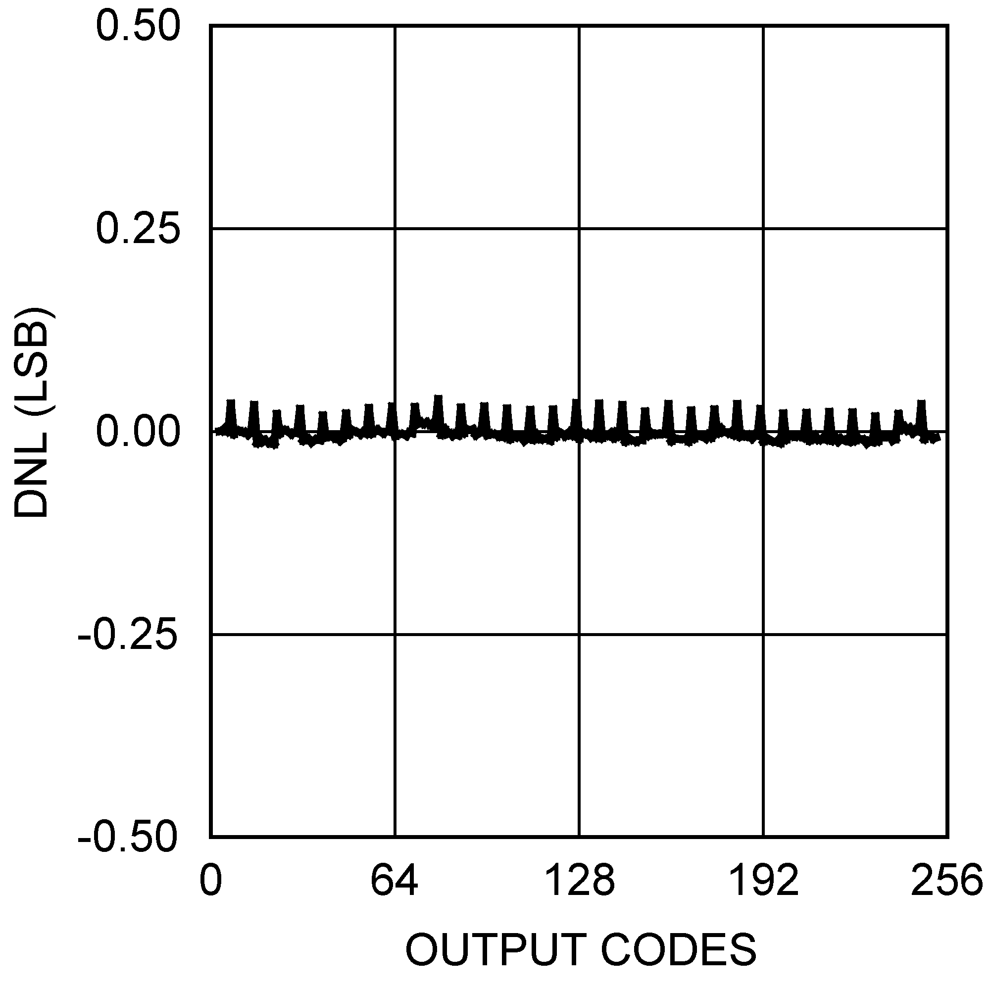
DNL vs Code at VA = 3 V

4 Revision History
Changes from E Revision (March 2013) to F Revision
- Added ESD Ratings table, Feature Description section, Device Functional Modes, Application and Implementation section, Power Supply Recommendations section, Layout section, Device and Documentation Support section, and Mechanical, Packaging, and Orderable Information section.Go
Changes from D Revision (March 2013) to E Revision
- Changed layout of National Data Sheet to TI formatGo