-
DAC101S101 and DAC101S101Q-1 10-Bit Micro Power, RRO Digital-to-Analog Converter SNAS321G June 2005 – April 2016 DAC101S101 , DAC101S101-Q1
PRODUCTION DATA.
-
DAC101S101 and DAC101S101Q-1 10-Bit Micro Power, RRO Digital-to-Analog Converter
- 1 Features
- 2 Applications
- 3 Description
- 4 Revision History
- 5 Description (continued)
- 6 Pin Configuration and Functions
- 7 Specifications
- 8 Detailed Description
- 9 Application and Implementation
- 10Power Supply Recommendations
- 11Layout
- 12Device and Documentation Support
- 13Mechanical, Packaging, and Orderable Information
- IMPORTANT NOTICE
DAC101S101 and DAC101S101Q-1 10-Bit Micro Power, RRO Digital-to-Analog Converter
1 Features
- DAC101S101Q is AEC-Q100 Grade 1 Qualified and is Manufactured on an Automotive Grade Flow.
- Ensured Monotonicity
- Low Power Operation
- Rail-to-Rail Voltage Output
- Power-on Reset to Zero Volts Output
- Wide Temperature Range of −40°C to +125°C
- Wide Power Supply Range of 2.7 V to 5.5 V
- Small Packages
- Power Down Feature
- Resolution 10 bits
- DNL +0.15, –0.05 LSB (typical)
- Output Settling Time 8 μs (typical)
- Zero Code Error 3.3 mV (typical)
- Full-Scale Error −0.06 %FS (typical)
- Power Consumption
- Normal Mode, 0.63 mW (3.6 V) / 1.41 mW (5.5 V) typical
- Power Down Mode, 0.14 μW (3.6 V) / 0.33 μW (5.5 V) typical
2 Applications
- Battery-Powered Instruments
- Digital Gain and Offset Adjustment
- Programmable Voltage & Current Sources
- Programmable Attenuators
- Automotive
3 Description
The DAC101S101 is a full-featured, general purpose 10-bit voltage-output digital-to-analog converter (DAC) that can operate from a single +2.7 V to 5.5 V supply and consumes just 175 µA of current at 3.6 Volts. The on-chip output amplifier allows rail-to-rail output swing and the three wire serial interface operates at clock rates up to 30 MHz over the specified supply voltage range and is compatible with standard SPI, QSPI, MICROWIRE and DSP interfaces. Competitive devices are limited to 20 MHz clock rates at supply voltages in the 2.7 V to 3.6 V range.
The supply voltage for the DAC101S101 serves as its voltage reference, providing the widest possible output dynamic range. A power-on reset circuit ensures that the DAC output powers up to zero volts and remains there until there is a valid write to the device. A power-down feature reduces power consumption to less than a microWatt.
Device Information(1)
| PART NUMBER | PACKAGE | BODY SIZE (NOM) |
|---|---|---|
| DAC101S101 | VSSOP (8) | 3.00 mm × 3.00 mm |
| DAC101S101, DAC101S101-Q1 |
SOT-23 (6) | 1.60 mm × 2.90 mm |
- For all available packages, see the orderable addendum at the end of the data sheet.
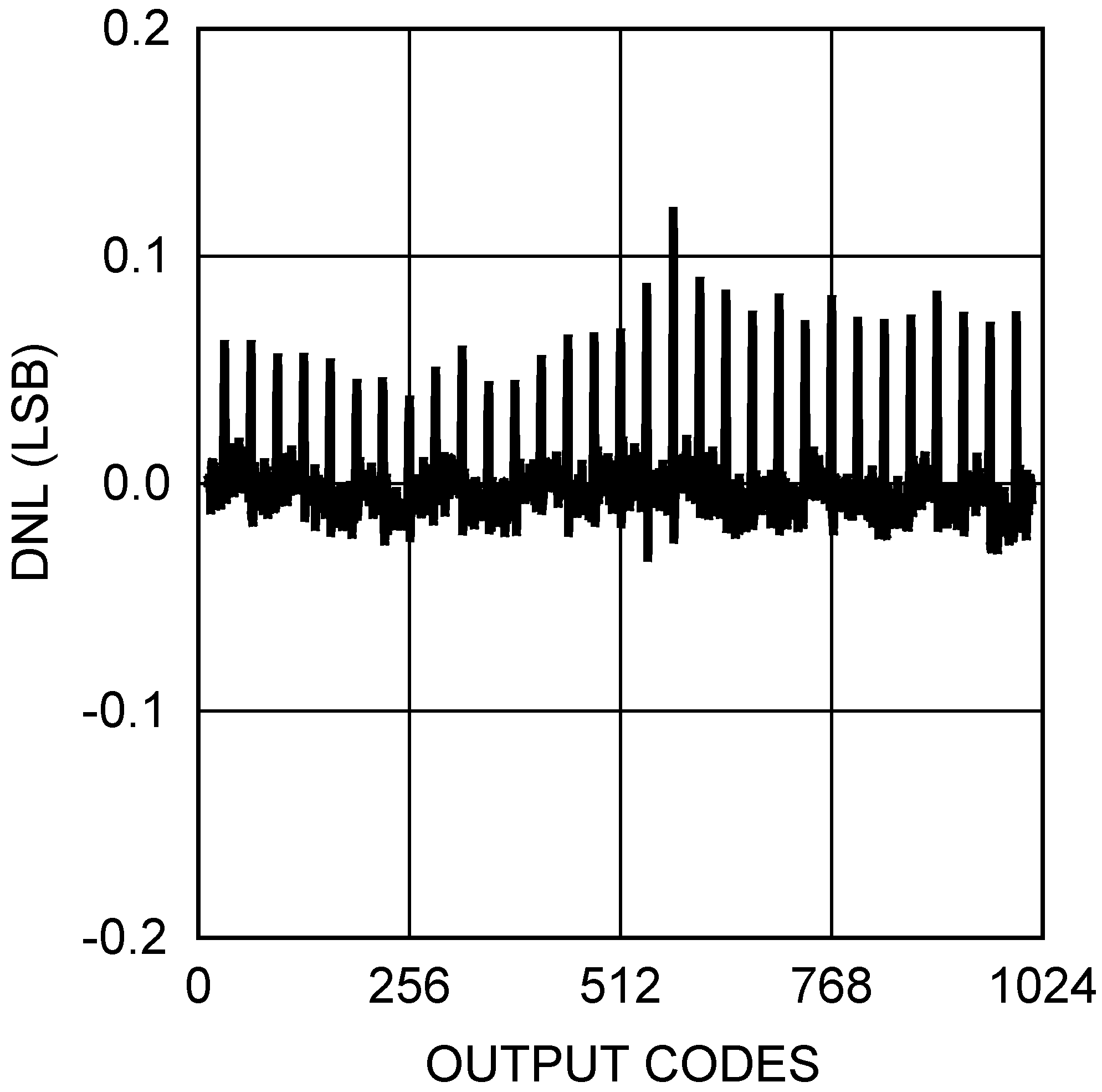
DNL at VA = 3 V
