DAC8532 Dual Channel, 16-Bit, Low Power, Serial Input Digital-To-Analog Converter
1 Features
- 16-Bit Monotonic Over Temperature
- MicroPower Operation: 500 µA at 5 V
- Power-On Reset to Zero-Scale
- Power Supply: 2.7 V to 5.5 V
- Settling Time: 10 µs to ±0.003% FSR
- Ultra-Low AC Crosstalk: –100 dB Typ
- Low-Power Serial Interface With
Schmitt-Triggered Inputs - On-Chip Output Buffer Amplifier With Rail-to-Rail Operation
- Double-Buffered Input Architecture
- Simultaneous or Sequential Output Update
and Powerdown - Available in a Tiny VSSOP-8 Package
2 Applications
- Portable Instrumentation
- Closed-Loop Servo Control
- Process Control
- Data Acquisition Systems
- Programmable Attenuation
- PC Peripherals
3 Description
The DAC8532 is a dual channel, 16-bit digital-to-analog converter (DAC) offering low power operation and a flexible serial host interface. Each on-chip precision output amplifier allows rail-to-rail output swing to be achieved over the supply range of 2.7 V to 5.5 V. The device supports a standard 3-wire serial interface capable of operating with input data clock frequencies up to 30 MHz for VDD = 5 V.
The DAC8532 requires an external reference voltage to set the output range of each DAC channel. The device incorporates a power-on reset circuit which ensures that the DAC outputs power up at zero-scale and remain there until a valid write takes place. The DAC8532 provides a flexible power-down feature, accessible over the serial interface, that reduces the current consumption of the device to 200 nA at 5 V.
The low-power consumption of the device in normal operation makes it ideally suited to portable battery-operated equipment and other low-power applications. The power consumption is 2.5 mW at 5 V, reducing to 1 µW in power-down mode.
The DAC8532 is available in a VSSOP-8 package with a specified operating temperature range of –40°C to 105°C.
Device Information(1)
| PART NUMBER | PACKAGE | BODY SIZE (NOM) |
|---|---|---|
| DAC8532 | VSSOP (8) | 3.00 mm × 3.00 mm |
- For all available packages, see the orderable addendum at the end of the datasheet.
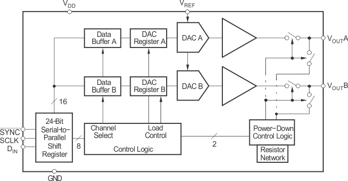
4 Simplified Diagram
5 Revision History
Changes from A Revision (May 2003) to B Revision
- Added Device Information and Handling Rating tables, Feature Description section, Device Functional Modes, Application and Implementation section, Power Supply Recommendations section, Layout section, Device and Documentation Support section, and Mechanical, Packaging, and Orderable Information section Go
Changes from * Revision (December 2001) to A Revision
- Added text string "No device pin should be brought high before power is applied to the device." to the Power-On Reset Description. Go
6 Pin Configuration and Functions
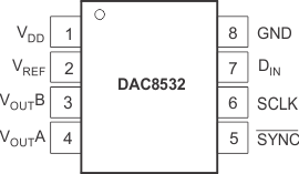
Pin Functions
| PIN | NAME | FUNCTION |
|---|---|---|
| 1 | VDD | Power supply input, 2.7 V to 5.5 V |
| 2 | VREF | Reference voltage input |
| 3 | VOUTB | Analog output voltage from DAC B |
| 4 | VOUTA | Analog output voltage from DAC A |
| 5 | SYNC | Level triggered SYNC input (active LOW). This is the frame synchronization signal for the input data. When SYNC goes LOW, it enables the input shift register and data is transferred on the falling edges of SCLK. The action specified by the 8-bit control byte and 16-bit data word is executed following the 24th falling SCLK clock edge (unless SYNC is taken HIGH before this edge in which case the rising edge of SYNC acts as an interrupt and the write sequence is ignored by the DAC8532). |
| 6 | SCLK | Serial Clock Input. Data can be transferred at rates up to 30 MHz at 5 V. |
| 7 | DIN | Serial Data Input. Data is clocked into the 24-bit input shift register on the falling edge of the serial clock input. |
| 8 | GND | Ground reference point for all circuitry on the part. |