SLES177B April 2006 – August 2015 PCM1808
PRODUCTION DATA.
- 1 Features
- 2 Applications
- 3 Description
- 4 Revision History
- 5 Pin Configuration and Functions
- 6 Specifications
- 7 Detailed Description
- 8 Application and Implementation
- 9 Power Supply Recommendations
- 10Layout
- 11Device and Documentation Support
- 12Mechanical, Packaging, and Orderable Information
1 Features
- 24-Bit Delta-Sigma Stereo A/D Converter (ADC)
- Single-Ended Voltage Input: 3 Vp-p
- High Performance:
- THD+N: –93 dB (Typical)
- SNR: 99 dB (Typical)
- Dynamic Range: 99 dB (Typical)
- Oversampling Decimation Filter:
- Oversampling Frequency: ×64
- Pass-Band Ripple: ±0.05 dB
- Stop-Band Attenuation: –65 dB
- On-Chip High-Pass Filter: 0.91 Hz (48 kHz)
- Flexible PCM Audio Interface
- Master- or Slave-Mode Selectable
- Data Formats: 24-Bit I2S, 24-Bit Left-Justified
- Power Down and Reset by Halting System Clock
- Analog Antialias LPF Included
- Sampling Rate: 8 kHz–96 kHz
- System Clock: 256 fS, 384 fS, 512 fS
- Resolution: 24 Bits
- Dual Power Supplies:
- 5-V for Analog
- 3.3-V for Digital
- Package: 14-Pin TSSOP
2 Applications
- DVD Recorder
- Digital TV
- AV Amplifier or Receiver
- MD Player
- CD Recorder
- Multitrack Receiver
- Electric Musical Instrument
3 Description
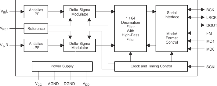
The PCM1808 device is a high-performance, low-cost, single-chip, stereo analog-to-digital converter with single-ended analog voltage input. The PCM1808 device uses a delta-sigma modulator with 64-times oversampling and includes a digital decimation filter and high-pass filter that removes the dc component of the input signal. For various applications, the PCM1808 device supports master and slave mode and two data formats in serial audio interface.
The PCM1808 device supports the power-down and reset functions by means of halting the system clock.
The PCM1808 device is suitable for wide variety of cost-sensitive consumer applications requiring good performance and operation with a 5-V analog supply and 3.3-V digital supply. Fabrication of the PCM1808 device uses a highly advanced CMOS process. The device is available in a small, 14-pin TSSOP package.
Device Information(1)
| PART NUMBER | PACKAGE | BODY SIZE (NOM) |
|---|---|---|
| PCM1808 | TSSOP (14) | 4.40 mm × 5.00 mm |
- For all available packages, see the orderable addendum at the end of the datasheet.
PCM1808 Block Diagram
