SNAU274 December 2021
1 ADC128S102EVM Overview
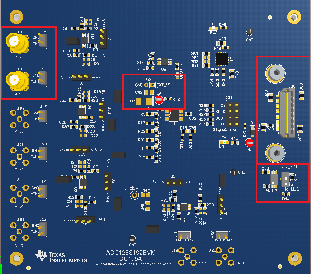
The ADC128S102EVM has provisions to drive all eight analog input channels, the external power supply, and the connection to the precision host interface (PHI) motherboard to communicate with the user-friendly GUI. These section are outlined in red in Figure 1-1. The final section is the EEPROM section below the J25 PHI connector. The switch, S1, must be in the WR_DIS position and must not be changed.
 Figure 1-1 ADC128S102EVM Board
Sections
Figure 1-1 ADC128S102EVM Board
SectionsTable 1-1 lists the related documents that are associated with the ADC128S102EVM.