SLLSE75B May 2011 – July 2016 TLK10002
PRODUCTION DATA.
- 1 Features
- 2 Applications
- 3 Description
- 4 Revision History
- 5 Description (continued)
- 6 Pin Configuration and Functions
-
7 Specifications
- 7.1 Absolute Maximum Ratings
- 7.2 ESD Ratings
- 7.3 Recommended Operating Conditions
- 7.4 Thermal Information
- 7.5 10-Gbps Power Characteristics - 1.0 V
- 7.6 10-Gbps Power Characteristics - 1.5 V
- 7.7 10-Gbps Power Characteristics - 1.8 V
- 7.8 Transmitter and Receiver Characteristics
- 7.9 MDIO Timing Requirements
- 7.10 JTAG Timing Requirements
- 7.11 Typical Characteristics
-
8 Detailed Description
- 8.1 Overview
- 8.2 Functional Block Diagram
- 8.3
Feature Description
- 8.3.1 High-Speed Side Receiver Jitter Tolerance
- 8.3.2 Lane Alignment Scheme
- 8.3.3 Lane Alignment Components
- 8.3.4 Lane Alignment Operation
- 8.3.5 Channel Synchronization
- 8.3.6 Line Rate, SERDES PLL Settings, and Reference Clock Selection
- 8.3.7 Clocking Architecture
- 8.3.8 Loopback Modes
- 8.3.9 Deep Remote Loopback
- 8.3.10 Shallow Remote Loopback and Serial Retime
- 8.3.11 Deep Local Loopback
- 8.3.12 Shallow Local Loopback
- 8.3.13 Test Pattern Generation and Verification
- 8.3.14 Latency Measurement Function
- 8.3.15 Power-Down Mode
- 8.3.16 High Speed CML Output
- 8.3.17 High Speed Receiver
- 8.3.18 Loss of Signal Indication (LOS)
- 8.3.19 MDIO Management Interface
- 8.3.20 MDIO Protocol Timing
- 8.3.21 Clause 22 Indirect Addressing
- 8.4 Device Functional Modes
- 8.5 Programming
- 8.6 Register Maps
- 9 Application and Implementation
- 10Power Supply Recommendations
- 11Layout
- 12Device and Documentation Support
- 13Mechanical, Packaging, and Orderable Information
1 Features
- Dual-Channel, 10-Gbps, Multi-Rate Transceiver
- Supports All CPRI and OBSAI Data Rates From 1 Gbps to 10 Gbps
- Integrated Latency Measurement Function, Accuracy up to 814 ps
- Supports SERDES Operation With up to 10-Gbps Data Rate on the High-Speed Side and up to 5G bps on the Low-Speed Side
- Differential CML I/Os on Both High-Speed and Low-Speed Sides
- Shared or Independent Reference Clock Per Channel
- Loopback Capability on Both High-Speed and Low-Speed Sides, OBSAI Compliant
- Supports Data Retime Operation
- Supports PRBS 27-1, 223-1 and 231-1 and High-Frequency, Low-Frequency, Mixed-Frequency, and CRPAT Long and Short Pattern Generation and Verification
- Two Power Supplies: 1-V Core, and 1.5-V or 1.8-V I/O
- Transmit De-Emphasis and Receive Adaptive Equalization to Allow Extended Backplane or Cable Reach on Both High-Speed and Low-Speed Sides
- Programmable Transmit Output Swing on Both High-Speed and Low-Speed Sides.
- Minimum Receiver Differential Input Threshold of 100 mVpp
- Loss-of-Signal (LOS) Detection
- Interface to Backplanes, Passive and Active Copper Cables, or SFP/SFP+ Optical Modules
- Hot Plug Protection
- JTAG; IEEE 1149.1 Test Interface
- MDIO; IEEE 802.3 Clause-22 Support
- 65-nm Advanced CMOS Technology
- Industrial Ambient Operating Temperature (–40°C to 85°C) at Full Rate
- Power Consumption: 1.6 W Typical
- Device Package: 13-mm × 13-mm, 144-pin PBGA, 1-mm Ball-Pitch
2 Applications
- Wireless Infrastructure CPRI and OBSAI Links
- High-Speed Video Applications
- Proprietary Cable or Backplane Links
- High-Speed Point-to-Point Transmission Systems
3 Description
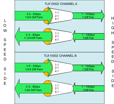
The TLK10002 device is a dual-channel, multi-rate transceiver intended for use in high-speed bidirectional point-to-point data transmission systems. It has special support for the wireless base station Remote Radio Head (RRH) application, but may also be used in other high-speed applications. It supports all the CPRI and OBSAI rates from 1.2288 Gbps to 9.8304 Gbps.
Device Information(1)
| PART NUMBER | PACKAGE | BODY SIZE (NOM) |
|---|---|---|
| TLK10002 | FCBGA (144) | 13.00 mm × 13.00 mm |
- For all available packages, see the orderable addendum at the end of the data sheet.
Simplified Schematic

4 Revision History
Changes from A Revision (July 2013) to B Revision
- Added ESD Ratings table, Feature Description section, Device Functional Modes, Application and Implementation section, Power Supply Recommendations section, Layout section, Device and Documentation Support section, and Mechanical, Packaging, and Orderable Information section.Go
Changes from * Revision (May 2011) to A Revision
- Changed Feature From: Supports all CPRI and OBSAI Data Rates To: Supports all CPRI and OBSAI Data Rates From 1Gbps to 10GbpsGo
- Changed Feature From: JTAG; IEEE 1149.1 /1149.6 Test Interface To: JTAG; IEEE 1149.1 Test InterfaceGo
- Changed JT1 and JD1 Parameters From: (CPRI LV/LV-II and OBSAI Rates) To: (CPRI LV/LV-II/ LV-III and OBSAI Rates)Go
- Changed JT2 and JD2 Parameters From: (CPRI E.6/12.HV) To: (CPRI E.12.HV)Go
- Deleted the RIN - Differential input impedance, MIN = 80 Ω and MAX = 120 Ω valuesGo
- Changed Functional Block Diagram text, From: 8B/10B Decoder Lane Align Master To: 8B/10B Encoder Lane Align MasterGo
- Changed text in the Lane Alignment Slave (LAS) section From: Resides in the TLK10002 LS transmitter To: Resides in the TLK10002 LS receiverGo
- Changed values in the text and in list item 1, From: 1.485Gbps To: 1.987Gbps and From: 2.97Gbps To: 3.974GbpsGo
- Changed list item 1 text From: "supported in the quarter rate mode (RateScale = 1)" To: "supported in the quarter rate mode (RateScale = 0.5)"Go
- Changed list item 4 text From: "clock frequencies can be selected: 148.5MHz, 185.625MHz, 247.5MHz, 297MHz, and 371.25MHz." To: "clock frequencies can be selected: 397.4MHz, 331.167MHz, 248.375MHz, 198.7MHz, 165.583MHz, 158.96MHz, and 132.467MHz."Go
- Changed Table 7Go
- Added list items for latency measurementGo
- Changed LOOPBACK_TP_CONTROL, BIT B.0 From: 1 = Enable shallow remote loopback mode To: Enable shallow local loopback modeGo
- Changed LAS_CONFIG_CONTROL BIT C.2 ACCESS From: RW To: RW SC(1)Go
- Deleted list item from the HS/LS Data Rate Setting section: "Write 1'B1 to 9.9 HS_PEAK_DISABLE (HS_OVERLAY_CONTROL = 0x0B00)."Go
- Changed list item in the HS Serial Configuration Changed section From: 4.11:10 (HS_CDRFMULT[1:0]), 4.9:8 (HS_CDRTHR[1:0]) To: 4.11:10 (HS_CDRFMULT[1:0]), 4.9:8 (HS_CDRTHR[1:0]), 4.5 (H1CDRMODE)Go
- Changed the HS/LS Data Rate Setting section: From: Refer to Table 3 To: Refer to Table 2Go
- Changed the HS/LS Data Rate Setting section: list item text Go