TPS54233 2A, 28V Input, Step Down DC/DC Converter With Eco-mode™
1 Features
- 3.5 V to 28 V Input Voltage Range
- Adjustable Output Voltage Down to 0.8 V
- Integrated 80 mΩ High Side MOSFET Supports up to 2A Continuous Output Current
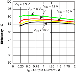
- High Efficiency at Light Loads with a Pulse Skipping Eco-mode™
- Fixed 300 kHz Switching Frequency
- Typical 1 μA Shutdown Quiescent Current
- Adjustable Slow Start Limits Inrush Currents
- Programmable UVLO Threshold
- Overvoltage Transient Protection
- Cycle by Cycle Current Limit, Frequency Fold Back and Thermal Shutdown Protection
- Available in Easy-to-Use SOIC8 Package
- Supported by WEBENCH® Software Tool (www.TI.com/WEBENCH)
2 Applications
- Consumer Applications such as Set-Top Boxes, CPE Equipment, LCD Displays, Peripherals, and Battery Chargers
- Industrial and Car Audio Power Supplies
- 5V, 12V and 24V Distributed Power Systems
3 Description
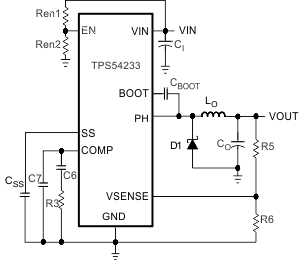
The TPS54233 is a 28 V, 2 A non-synchronous buck converter that integrates a low RDS(on) high side MOSFET. To increase efficiency at light loads, a pulse skipping Eco-mode™ feature is automatically activated. Furthermore, the 1 μA shutdown supply current allows the device to be used in battery powered applications. Current mode control with internal slope compensation simplifies the external compensation calculations and reduces component count while allowing the use of ceramic output capacitors. A resistor divider programs the Hysteresis of the input under-voltage lockout. An overvoltage transient protection circuit limits voltage overshoots during startup and transient conditions. A cycle by cycle current limit scheme, frequency fold back and thermal shutdown protect the device and the load in the event of an overload condition. The TPS54233 is available in an 8-pin SOIC package that has been internally optimized to improve thermal performance.
Device Information(1)
| PART NUMBER | PACKAGE | BODY SIZE (NOM) |
|---|---|---|
| TPS54233 | SOIC (8) | 4.90 mm x 3.90 mm |
- For all available packages, see the orderable addendum at the end of the data sheet.
5 Revision History
Changes from B Revision (February 2011) to C Revision
- Added ESD Rating table, Thermal Information table, Feature Description section, Device Functional Modes, Application and Implementation section, Power Supply Recommendations section, Device and Documentation Support section, and Mechanical, Packaging sections. Go
- Deleted Features Item: For SWIFT™ Documentation, See the TI Website at www.ti.com/swiftGo
- Changed Features item: Supported by SwitcherPro™ To: Supported by WEBENCH®Go
- Changed RO1 To: R5, RO2 To R6, C1 To C6, and C2 To C7 in the Simplified SchematicGo
- Changed SwitcherPro™ Software tool To: WEBENCH Software tool in the Current Mode Compensation Design sectionGo
- Changed RO1 To: R5, RO2 To R6, C1 To C6, and C2 To C7 in the Table 1Go
- Changed the Output Voltage Set Point section. Updated the paragraph following Equation 5.Go
Changes from A Revision (March 2010) to B Revision
Changes from * Revision (October 2008) to A Revision
- Changed the Absolute Maximum Ratings table, Input Voltage - EN pin max value From: 5V to 6VGo
- Added A table to the Description - with text "For additional design needs, see.."Go
6 Pin Configuration and Functions
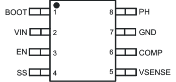
Pin Functions
| PIN | DESCRIPTION | |
|---|---|---|
| NAME | NO. | |
| BOOT | 1 | A 0.1 μF bootstrap capacitor is required between BOOT and PH. If the voltage on this capacitor falls below the minimum requirement, the high-side MOSFET is forced to switch off until the capacitor is refreshed. |
| VIN | 2 | Input supply voltage, 3.5 V to 28 V. |
| EN | 3 | Enable pin. Pull below 1.25V to disable. Float to enable. Programming the input undervoltage lockout with two resistors is recommended. |
| SS | 4 | Slow start pin. An external capacitor connected to this pin sets the output rise time. |
| VSENSE | 5 | Inverting node of the gm error amplifier. |
| COMP | 6 | Error amplifier output, and input to the PWM comparator. Connect frequency compensation components to this pin. |
| GND | 7 | Ground. |
| PH | 8 | The source of the internal high-side power MOSFET. |
7 Specifications
7.1 Absolute Maximum Ratings(1)
over operating free-air temperature range (unless otherwise noted)7.2 ESD Ratings
| VALUE | UNIT | |||
|---|---|---|---|---|
| V(ESD) | Electrostatic discharge | Human-body model (HBM), per ANSI/ESDA/JEDEC JS-001(1) | ±2000 | V |
| Charged-device model (CDM), per JEDEC specification JESD22-C101(2) | ±500 | |||
7.3 Recommended Operating Conditions
over operating free-air temperature range (unless otherwise noted)| MIN | TYP | MAX | UNIT | |
|---|---|---|---|---|
| Operating Input Voltage on (VIN pin) | 3.5 | 28 | V | |
| Operating junction temperature, TJ | –40 | 150 | °C |
7.4 Thermal Information
| THERMAL METRIC(1) | D | UNIT | |
|---|---|---|---|
| 8 PINS | |||
| RθJA | Junction-to-ambient thermal resistance | 116.7 | °C/W |
| RθJC(top) | Junction-to-case (top) thermal resistance | 62.4 | |
| RθJB | Junction-to-board thermal resistance | 57.0 | |
| ψJT | Junction-to-top characterization parameter | 14.5 | |
| ψJB | Junction-to-board characterization parameter | 56.5 | |
| RθJC(bot) | Junction-to-case (bottom) thermal resistance | N/A | |
7.5 Electrical Characteristics
TJ = –40°C to 150°C, VIN = 3.5V to 28V (unless otherwise noted)| PARAMETER | TEST CONDITIONS | MIN | TYP | MAX | UNIT |
|---|---|---|---|---|---|
| SUPPLY VOLTAGE (VIN PIN) | |||||
| Internal undervoltage lockout threshold | Rising and Falling | 3.5 | V | ||
| Shutdown supply current | EN = 0V, VIN = 12V, –40°C to 85°C | 1 | 4 | μA | |
| Operating – non switching supply current | VSENSE = 0.85 V | 75 | 110 | μA | |
| ENABLE AND UVLO (EN PIN) | |||||
| Enable threshold | Rising and Falling | 1.25 | 1.35 | V | |
| Input current | Enable threshold – 50 mV | -1 | μA | ||
| Input current | Enable threshold + 50 mV | -4 | μA | ||
| VOLTAGE REFERENCE | |||||
| Voltage reference | 0.772 | 0.8 | 0.828 | V | |
| HIGH-SIDE MOSFET | |||||
| On resistance | BOOT-PH = 3 V, VIN = 3.5 V | 115 | 200 | mΩ | |
| BOOT-PH = 6 V, VIN = 12 V | 80 | 150 | |||
| ERROR AMPLIFIER | |||||
| Error amplifier transconductance (gm) | –2 μA < I(COMP) < 2 μA, V(COMP) = 1 V | 92 | μmhos | ||
| Error amplifier DC gain(1) | VSENSE = 0.8 V | 800 | V/V | ||
| Error amplifier unity gain bandwidth(1) | 5 pF capacitance from COMP to GND pins | 2.7 | MHz | ||
| Error amplifier source/sink current | V(COMP) = 1 V, 100 mV overdrive | ±7 | μA | ||
| Switch current to COMP transconductance | VIN = 12 V | 9 | A/V | ||
| PULSE SKIPPING Eco-mode™ | |||||
| Pulse skipping Eco-mode™ switch current threshold | 100 | mA | |||
| CURRENT LIMIT | |||||
| Current limit threshold | VIN = 12 V | 2.3 | 3.5 | A | |
| THERMAL SHUTDOWN | |||||
| Thermal Shutdown | 165 | °C | |||
| SLOW START (SS PIN) | |||||
| Charge current | V(SS) = 0.4 V | 2 | μA | ||
| SS to VSENSE matching | V(SS) = 0.4 V | 10 | mV | ||
7.6 Switching Characteristics
TJ = –40°C to 150°C, VIN = 3.5 to 28 V (unless otherwise noted)| PARAMETER | TEST CONDITIONS | MIN | TYP | MAX | UNIT | |
|---|---|---|---|---|---|---|
| SWITCHING FREQUENCY | ||||||
| Device switching frequency | VIN = 12 V | 210 | 300 | 390 | kHz | |
| Minimum controllable on time | VIN = 12 V, 25°C | 105 | 130 | ns | ||
| Maximum controllable duty ratio(1) | BOOT-PH = 6 V | 90% | 93% | |||
7.7 Typical Characteristics
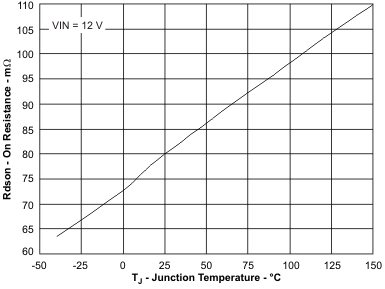 Figure 1. On Resistance vs Junction Temperature
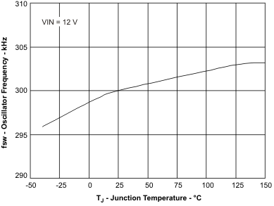 Figure 3. Switching Frequency vs Junction Temperature
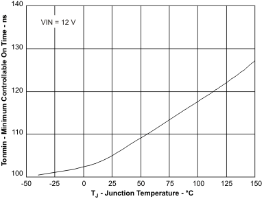 Figure 5. Minimum Controllable On Time vs
 Junction Temperature
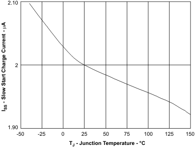 Figure 7. SS Charge Current vs Junction Temperature
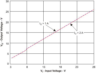 Figure 9. Typical Maximum Output Voltage vs
 Input Voltage
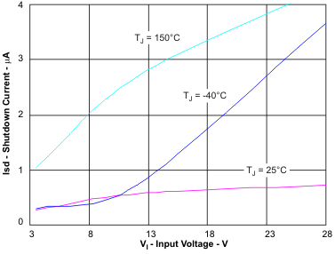 Figure 2. Shutdown Quiescent Current vs Input Voltage
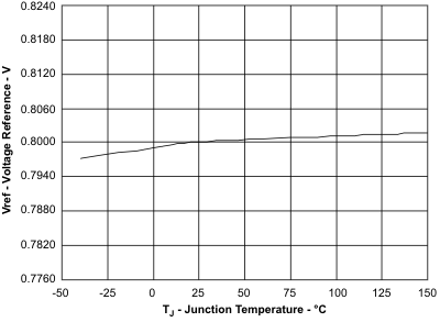 Figure 4. Voltage Reference vs Junction Temperature
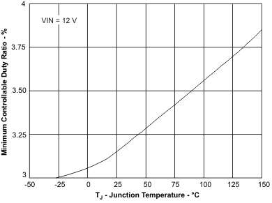 Figure 6. Minimum Controllable Duty Ratio vs
 Junction Temperature
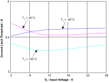 Figure 8. Current Limit Threshold vs Input Voltage
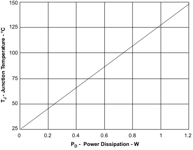 Figure 10. Maximum Power Dissipation vs
 Junction Temperature