SNVSA52E August 2014 – September 2016
PRODUCTION DATA.
- 1 Features
- 2 Applications
- 3 Description
- 4 Revision History
- 5 Device Comparison Table
- 6 Pin Configuration and Functions
- 7 Specifications
-
8 Detailed Description
- 8.1 Overview
- 8.2 Functional Block Diagram
- 8.3 Feature Description
- 8.4 Device Functioning Modes
- 8.5 Programming
- 8.6
Register Descriptions
- 8.6.1 Enable Register (0x01)
- 8.6.2 IVFM Register (0x02)
- 8.6.3 LED1 Flash Brightness Register (0x03)
- 8.6.4 LED2 Flash Brightness Register (0x04)
- 8.6.5 LED1 Torch Brightness Register (0x05)
- 8.6.6 LED2 Torch Brightness Register (0x06)
- 8.6.7 Boost Configuration Register (0x07)
- 8.6.8 Timing Configuration Register (0x08)
- 8.6.9 TEMP Register (0x09)
- 8.6.10 Flags1 Register (0x0A)
- 8.6.11 Flags2 Register (0x0B)
- 8.6.12 Device ID Register (0x0C)
- 8.6.13 Last Flash Register (0x0D)
- 9 Applications and Implementation
- 10Power Supply Recommendations
- 11Layout
- 12Device and Documentation Support
- 13Mechanical, Packaging, and Orderable Information
1 Features
- Dual Independent 1.5-A LED Current Source Programmability
- Accurate and Programmable LED Current Range from 1.4 mA to 1.5 A
- Torch Currents up to 360 mA (LM3644TT)
- Flash Timeout Values up to 1.6 seconds (LM3644TT)
- Optimized Flash LED Current During Low Battery Conditions (IVFM)
- > 85% Efficiency in Torch Mode (at 100 mA) and Flash Mode (at 1 A to 1.5 A)
- Grounded Cathode LED Operation for Improved Thermal Management
- Small Solution Size: < 16 mm2
- Hardware Strobe Enable (STROBE)
- Synchronization Input for RF Power Amplifier Pulse Events (TX)
- Hardware Torch Enable (TORCH/TEMP)
- Remote NTC Monitoring (TORCH/TEMP)
- 400-kHz I2C-Compatible Interface
- LM3644 (I2C Address = 0x63)
2 Applications
3 Description
The LM3644 is a dual LED flash driver that provides a high level of adjustability within a small solution size. The LM3644 utilizes a 2-MHz or 4-MHz fixed-frequency synchronous boost converter to provide power to the dual 1.5-A constant current LED sources. The dual 128 level current sources provide the flexibility to adjust the current ratios between LED1 and LED2. An adaptive regulation method ensures the current sources remain in regulation and maximizes efficiency.
Features of the LM3644 are controlled via an I2C-compatible interface. These features include: hardware flash and hardware torch pins (STROBE and TORCH/TEMP), a TX interrupt, and an NTC thermistor monitor. The device offers independently programmable currents in each output leg to drive the LEDs in a Flash or Movie Mode (Torch) condition.
The 2-MHz or 4-MHz switching frequency options, overvoltage protection (OVP), and adjustable current limit allow for the use of tiny, low-profile inductors and 10-µF ceramic capacitors. The device operates over a –40°C to +85°C ambient temperature range.
Device Information(1)
| PART NUMBER | PACKAGE | BODY SIZE (MAX) |
|---|---|---|
| LM3644 | DSBGA (12) | 1.69 mm x 1.31 mm |
- For all available packages, see the orderable addendum at the end of the data sheet.
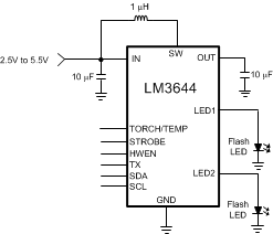
Simplified Schematic
